
Transistor
Question 1. For a CE transistor amplifier, the audio-signal voltage across the collector resistor of 2 kΩ resistance is 4 V. The current-amplification factor of the transistor is 100 and the base resistance is1 kΩ then the input-signal voltage is
- 10 mV
- 20 mV
- 30 mV
- 15 mV
Answer: 2. 20 mV
The voltage gain (or voltage amplification) is given by
⇒ \(A_v=\frac{\text { output voltage }\left(V_{\mathrm{o}}\right)}{\text { input voltage }\left(V_{\mathrm{i}}\right)}\)
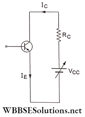
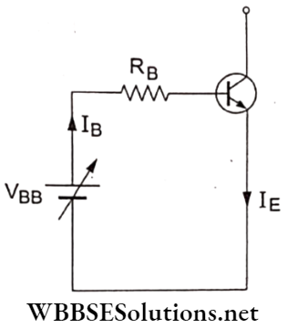
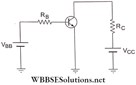
⇒ \(A_v=\frac{I_C R_C}{I_B R_B}\) → (1)
Given that collector resistance = Rc = 2 kΩ,
current amplification factor = \(\beta=\frac{I_{\mathrm{C}}}{I_{\mathrm{B}}}=100\),
base resistance = RB = 1 kΩ
and output voltage = Vo = 4V.
From (1),
⇒ \(A_v=\beta\left(\frac{R_{\mathrm{C}}}{R_{\mathrm{B}}}\right)=100 \times \frac{2 \mathrm{k} \Omega}{1 \mathrm{k} \Omega}=200\)
∵ \(A_v=\frac{V_{\mathrm{o}}}{V_{\mathrm{i}}}=200\)
∴ input voltage = \(V_{\mathrm{i}}=\frac{V_{\mathrm{o}}}{200}=\frac{4 \mathrm{~V}}{200}=20 \mathrm{mV}\).

Question 2. In a CE transistor amplifier, the audio-signal voltage across the collector is 3 V. The resistance of the collector is 3 kΩ. If the current gain is 100 and the base resistance is 2 kΩ, the voltage and power gains of the amplifier are respectively
- 200 and 1000
- 15 and 200
- 150 and 15000
- 20 and 2000
Answer: 3. 150 and 15000
Given that voltage across the collector = output voltage = Vo = 3 V,
collector resistance = output load = Ro = 3 kΩ,
is transistor in neet syllabus 2023
current gain = β =Io/Ii =100 .
and input resistance = base resistance = Ri = 2 kΩ.
∴ voltage gain = \(\frac{V_{\mathrm{o}}}{V_{\mathrm{i}}}=\frac{I_{\mathrm{o}} R_{\mathrm{o}}}{I_{\mathrm{i}} R_{\mathrm{i}}}=\beta\left(\frac{3 \mathrm{k} \Omega}{2 \mathrm{k} \Omega}\right)=100 \times 1.5=150\)
Now, power gain = (current gain)(voltage gain)
∴ \(\beta\left(\frac{V_{\mathrm{o}}}{V_{\mathrm{i}}}\right)=100 \times 150=1500\)
Read And Learn Also NEET Physics Multiple Choice Question and Answers
Question 3. A transistor is operated in the common-emitter configuration at Vc = 2 V such that a change in the base current from 100 μA to 200 μA produces a change in the collector current from 5 mA to 10 mA. The current gain is
- 150
- 75
- 50
- 100
Answer: 3. 50
The change in the base current is ΔIB = 200 μA-100 μA =100 μA.
The corresponding change in the collector current is
ΔIC=10 mA- 5 mA = 5 mA.
By definition,
∴ current gain = \(\beta=\frac{\Delta I_{\mathrm{C}}}{\Delta I_{\mathrm{B}}}=\frac{5 \mathrm{~mA}}{100 \mu \mathrm{A}}=\frac{5 \times 10^{-3}}{100 \times 10^{-6}}=\frac{5000}{100}=50\)
Question 4. A transistor is operated in the CE configuration at a constant collector voltage of Vc =15 V such that a change in the base current from 100 μA to 150 μA produces a change in the collector current from 5 mA to 10 mA. The current gain β is
- 75
- 50
- 100
- 67
Answer: 3. 100
Given that ΔIB =150 μA – 100 μA = 50 μA.
The corresponding collector current is ΔIC = 10 mA – 5 mA = 5 mA
∴ current gain = \(\beta=\frac{\Delta I_C}{\Delta I_B}=\frac{5 m A}{50 \mu \mathrm{A}}=100\)
Question 5. An n-p-n transistor is connected in the common-emitter (CE) configuration in a given amplifier. A load resistor of resistance 800 Ω, is connected in the collector circuit, and the voltage drop across it is 0.8 V. If the current-amplification factor is 0.96 and the input resistance of the circuit is 192 Ω, the voltage gain and the power gain of the amplifier will respectively be
- 3.69 and 3.84
- 4 and 3.84
- 4 and 4
- 4 and 3.69
Answer: 2. 4 and 3.84
Given that load resistance = Ro = 800 Ω,
voltage drop across the load = Vo = 0.8 V,
current amplification factor = \(\beta=\frac{I_C}{I_B}=0.96\)
and input resistance = RB = 192 Ω.
∴ voltage gain = \(\frac{V_0}{V_{\mathrm{i}}}=\frac{I_{\mathrm{C}} R_{\mathrm{C}}}{I_{\mathrm{B}} R_{\mathrm{B}}}=\left(\frac{800 \Omega}{192 \Omega}\right)(0.96)=4\)
Hence, power gain = (current gain)(voltage gain)
∴ \(\left(\frac{I_{\mathrm{C}}}{I_{\mathrm{B}}}\right)\left(\frac{V_{\mathrm{o}}}{V_{\mathrm{i}}}\right)=\beta\left(\frac{V_{\mathrm{o}}}{V_{\mathrm{I}}}\right)=0.96 \times 4=3.84\)
Question 6. For a transistor with Ic/IE = 0.96, the current gain in the common emitter configuration is
- 12
- 48
- 24
- 6
Answer: 3. 24
In a transistor,
⇒ \(I_{\mathrm{E}}=I_{\mathrm{C}}+I_{\mathrm{B}}\)
⇒ \(\frac{I_{\mathrm{E}}}{I_{\mathrm{C}}}=1+\frac{I_{\mathrm{B}}}{I_{\mathrm{C}}}\)
⇒ \(\frac{1}{0.96}=1+\frac{I_{\mathrm{B}}}{I_{\mathrm{C}}} \Rightarrow \frac{I_{\mathrm{B}}}{I_{\mathrm{C}}}=\frac{4}{96}=\frac{1}{24}\)
∴ current gain = \(\frac{I_{\mathrm{C}}}{I_{\mathrm{B}}}=24\)
Question 7. The correct relationship of the two current gains a and p in a transistor is
- \(\beta=\frac{1+\alpha}{\beta}\)
- \(\alpha=\frac{\beta}{1+\beta}\)
- \(\alpha=\frac{\beta}{1-\beta}\)
- \(\beta=\frac{\alpha}{1+\alpha}\)
Answer: 2. \(\alpha=\frac{\beta}{1+\beta}\)
In a transistor,
⇒ \(\alpha=\frac{I_{\mathrm{C}}}{I_{\mathrm{E}}} \text { and } \beta=\frac{I_{\mathrm{C}}}{I_{\mathrm{B}}}\)
Now, emitter current = collector current + base current
⇒ \(I_{\mathrm{E}}=I_{\mathrm{C}}+I_{\mathrm{B}}\)
⇒ \(\frac{I_{\mathrm{E}}}{I_{\mathrm{C}}}=1+\frac{I_{\mathrm{B}}}{I_{\mathrm{C}}} \Rightarrow \frac{1}{\alpha}=1+\frac{1}{\beta}=\frac{\beta+1}{\beta}\)
∴ \(\alpha=\frac{\beta}{1+\beta}\).
Question 8. In the common-base configuration of a transistor, ΔIc/ΔIE = 0.98. Then, the current gain in the common-emitter configuration of the transistor will be
- 98
- 24.5
- 4.9
- 49
Answer: 4. 49
In the common-base configuration, the current gain is given by
⇒ \(\alpha=\frac{\Delta I_{\mathrm{C}}}{\Delta I_{\mathrm{E}}}=0.98\)
In the common-emitter configuration, the current gain is given by
is transistor in neet syllabus 2023
⇒ \(\beta=\frac{\Delta I_{\mathrm{C}}}{\Delta I_{\mathrm{B}}}=\frac{\Delta I_{\mathrm{C}}}{\Delta I_{\mathrm{E}}-\Delta I_{\mathrm{C}}}\) [∵IE = IC + IB]
∴ \(\frac{1}{\frac{\Delta I_{\mathrm{E}}}{\Delta I_{\mathrm{C}}}-1}=\frac{1}{\frac{1}{\alpha}-1}=\frac{\alpha}{1-\alpha}=\frac{0.98}{1-0.98}=\frac{0.98}{0.02}=49\)
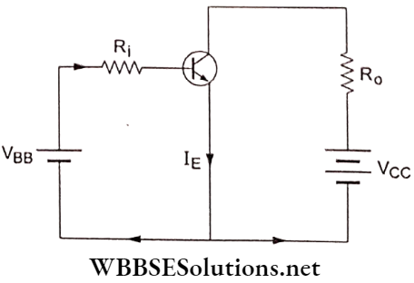
Question 9. In the circuit shown in the adjoining figure, when the input voltage of the base resistance is 10 V, VBE is zero, and VCE is also zero. The value of β is
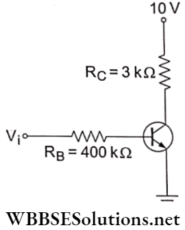
- 196
- 154
- 105
- 133
Answer: 4. 133
Given that input voltage = Vi =10 V and base resistance = RB = 400 kΩ = 400 x l03 Ω; the load resistance in the collector circuit is Rc = 3 kΩ = 3 x 10³ Ω. Also, VBE = 0 V, VCE = 0 V, and VCC =10 V.
∴ Vi – VBE = RBIB ⇒ 10 V – 0 V = (400 x 103 Ω.)IB.
∴ base current = \(I_{\mathrm{B}}=\frac{10 \mathrm{~V}}{4 \times 10^5 \Omega}=25 \mu \mathrm{A}\)
Again, in the output circuit,
⇒ \(V_{\mathrm{CC}}-V_{\mathrm{CE}}=I_{\mathrm{C}} R_{\mathrm{C}}\)
⇒ \(I_{\mathrm{C}}=\frac{V_{\mathrm{CC}}-V_{\mathrm{CE}}}{R_{\mathrm{C}}}=\frac{10 \mathrm{~V}-0 \mathrm{~V}}{3 \times 10^3 \Omega}=\frac{10 \mathrm{~V}}{3 \times 10^3 \Omega}=3.33 \mathrm{~mA}\)
∴ \(\beta=\frac{I_{\mathrm{C}}}{I_{\mathrm{B}}}=\frac{3.33 \mathrm{~mA}}{25 \mu \mathrm{A}}=\frac{3.33}{25} \times 10^3=133\)
Question 10. An amplifier has a voltage gain of Av = 1000. The voltage gain in dB is
- 20 dB
- 60 dB
- 3 dB
- 30 dB
Answer: 2. 60 dB
Voltage gain = (20 log Av) dB = (20 log 1000) dB
= (20 log 103) dB = 60 dB.
Question 11. Which of the following statements about a transistor is not true?
- The emitter is heavily doped.
- The base is thin.
- The base is lightly doped.
- The collector region is smaller compared to the emitter region in size.
Answer: 4. The collector region is smaller compared to the emitter region in size.
In a transistor, the middle layer called the base, is very thin (width ≈1 μm) and very lightly doped. The emitter is heavily doped and the collector is moderately doped. As regards the contact area, the collector has a comparatively larger area than the base and the emitter.
Question 12. In the given figure, an n-p-n transistor in the common-emitter configuration has a current gain of β = 100. The output voltage (Vo) of the amplifier will be
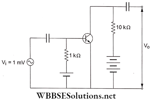
- 10 V
- 10 mV
- 1.0 V
- 0.1 V
Answer: 3. 1.0 V
Given that current gain = \(\beta=\frac{I_{\mathrm{C}}}{I_{\mathrm{B}}}=100\)
input resistance = RB = 1 kΩ,
and output load resistance = RC =10 kΩ.
Now, base current = \(\frac{\text { input voltage }}{\text { input resistance }}\)
⇒ \(I_B=\frac{1.0 \mathrm{mV}}{1 \mathrm{k} \Omega}=\frac{1.0 \times 10^{-3} \mathrm{~V}}{1 \times 10^3 \Omega}=1.0 \times 10^{-6} \mathrm{~A}\)
∴ collector current = IC = βIB = 100 x 10-6 A = 10-4 A.
Hence, output voltage = Vc = ICRC = (10-4 A)(10 kΩ)
= (10-4 A)(104 Ω) = 1.0 V.
| Class 11 Physics | Class 12 Maths | Class 11 Chemistry |
| NEET Foundation | Class 12 Physics | NEET Physics |
Question 13. A transistor connected in the common-emitter mode contains a load resistance of 5 kΩ and an input resistance of 1 kΩ. If the input peak voltage is 5 mV and the current gain is 50, find the voltage gain.
- 500
- 50
- 250
- 125
Answer: 3. 250
Given that load resistance = RC = 5 kΩ,
input resistance = Ri = 1 kΩ, input voltage = Vi = 5 mV,
and current gain = β = 50.
∴ voltage gain = \(A_v=\frac{\text { output voltage across } \mathrm{R}_{\mathrm{C}}}{\text { input voltage }}\)
∴ \(\frac{R_{\mathrm{C}} I_{\mathrm{C}}}{R_{\mathrm{i}} I_{\mathrm{B}}}=\beta\left(\frac{R_{\mathrm{C}}}{R_{\mathrm{i}}}\right)=50\left(\frac{5 \mathrm{k} \Omega}{1 \mathrm{k} \Omega}\right)=250\).
Question 14. The current gain for a transistor working as a common-base amplifier is 0.96. If the emitter current is 7.2 ma, the base current is
- 0.39 mA
- 0.43 mA
- 0.29 mA
- 0.35 mA
Answer: 3. 0.29 mA
In the common-base configuration,
current gain = \(\alpha=\frac{I_{\mathrm{C}}}{I_{\mathrm{E}}}=0.96\)
Given that IE = 7.2 mA. Hence, collector current = IC = 0.96 x 7.2 mA.
∴ base current = IB = IE– IC
is transistor in neet syllabus 2023
= 7.2 mA -0.96(7.2 mA)
= (7.2 mA)(l-0.96) = (7.2 mA)(0.04)
= 0.288 mA ~ 0.29 mA.
Question 15. For a common-emitter transistor, the input current is 5 pA, the voltage gain is β = 100, and the circuit is operated at a load resistance of 10 kΩ. The voltage between the collector and the emitter will be
- 12.5 V
- 5 V
- 7.5 V
- 10 V
Answer: 2. 5 V
Given that input current = IB = 5 μA, current gain = β =100, and load resistance = RC = 10 kΩ.
∵ \(\beta=\frac{I_{\mathrm{C}}}{I_{\mathrm{B}}}=100\),
∴collector current = IC = 100IB = 100(5 μA) = 500 μA.
∴ output voltage = ICRC = (500 μA)(10 kΩ)
= 500 x 10-6 x 10 x 103 V = 5 V.
Question 16. Consider an n-p-n transistor amplifier in the common-emitter mode. The current gain of the transistor is 100. If the collector current changes by 1 mA, what will be the change in the emitter current?
- 1.1mA
- 1.01mA
- 10 mA
- 0.01mA
Answer: 2. 1.01mA
For an n-p-n transistor in the CE mode,
current gain = \(\beta=\frac{\Delta I_{\mathrm{C}}}{\Delta I_{\mathrm{B}}} \Rightarrow 100=\frac{1 \mathrm{~mA}}{\Delta I_{\mathrm{B}}}\)
∴ the change in the base current will be
⇒ \(\Delta I_{\mathrm{B}}=\frac{1 \mathrm{~mA}}{100}=0.01 \mathrm{~mA}\)
Hence, the change in the emitter current will be
∴ ΔIE = ΔIC + ΔIB = 1 mA + 0.01 mA = 1.01 mA.
Question 17. If the collector current is 120 mA, the base current is 2 mA, and the resistance gain is 3, what is the power gain?
- 180
- 10800
- 1.8
- 18
Answer: 2. 10800
Current gain = \(\beta=\frac{I_{\mathrm{C}}}{I_{\mathrm{B}}}=\frac{120 \mathrm{~mA}}{2 \mathrm{~mA}}=60\)
∴ power gain = β2 x resistance gain = 602 x 3 = 10800.
Question 18. In a common-base amplifier, the phase difference between the input-signal voltage and the output voltage is
- zero
- \(\frac{\pi}{2}\)
- \(\frac{\pi}{4}\)
- π
Answer: 1. zero
In a transistor amplifier in the CB configuration, the input and output voltages are in the same phase. So, the phase difference is zero.
Question 19. To use a transistor as an amplifier,
- The emitter-base junction is forward-biased and the base-collector junction is reverse-biased
- No bias voltages are required
- Both junctions are forward-biased
- Both junctions are reverse-biased
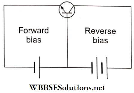
Answer: 1. The emitter-base junction is forward-biased and the base-collector junction is reverse-biased
The adjoining figure shows an n-p-n transistor in the CB configuration as an amplifier. This is used when a low input impedance is required. Due to the forward bias in the input, the base-emitter junction acts as a forward-biased p-n junction diode and has a low input impedance. The output across the base-collector junction acts as a reversed-biased junction diode. Hence, a common base amplifier has a high output impedance. An amplifier with a low input impedance and a high output impedance provides a high voltage gain.
Question 20. When an n-p-n transistor is used as an amplifier,
- Holes move from the emitter to the base
- Holes move from the base to the emitter
- Electrons move from the collector to the base
- Electrons move from the base to the collector
Answer: 4. Electrons move from the base to the collector
As shown in the diagram of the preceding question, collector current(Ic) has been shown to flow from the collector to the base. Hence, electrons move from the base to the collector.
Question 21. The voltage gain (Av) of the given amplifier is
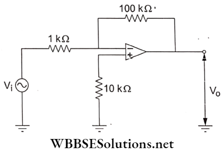
- 1000
- 100
- 10
- 9.9
Answer: 2. 100
The voltage gain in an operational amplifier is given by
⇒ \(A_v=\frac{V_{\mathrm{o}}}{V_{\mathrm{i}}}=\frac{R_{\mathrm{f}}}{R_{\mathrm{i}}}\)
∴ \(A_v=\frac{100 \mathrm{k} \Omega}{1 \mathrm{k} \Omega}=100\).
Question 22. The transfer ratio p of a transistor is 50. The input resistance of the transistor when used in the common-emitter configuration is 1 kΩ. The peak value of the collector AC current for an AC input voltage of 0.01 V peak is
- 100 μA
- 0.01 mA
- 0.25 mA
- 500 μA
Answer: 4. 500 μA
Given that input resistance = \(R_{\mathrm{B}}=1 \mathrm{k} \Omega\)
and base current = \(I_{\mathrm{B}}=\frac{V_{\mathrm{B}}}{R_{\mathrm{B}}}=\frac{0.01 \mathrm{~V}}{1000 \Omega}=10^{-5} \mathrm{~A}\)
Now, \(\beta=\frac{I_{\mathrm{C}}}{I_{\mathrm{B}}} \Rightarrow 50=\frac{I_{\mathrm{C}}}{10^{-5} \mathrm{~A}}\)
∴ collector current = Ic = 50 x 10-5 A = 500 x 10-6 A = 500 μA.
Question 23. An oscillator is nothing but an amplifier with
- A positive feedback
- A negative feedback
- A large gain
- No feedback
Answer: 1. A positive feedback
In an oscillator, part of the output signal is fed back to the amplifier input in such a way that the feedback signal is regenerated, reamplified, and fed back again to maintain a constant output signal. Hence, an oscillator is an amplifier with a positive feedback
Question 24. The input signal given to a CE amplifier Physics having a voltage gain of 150 is
\(V_{\mathrm{i}}=(2 \mathrm{~V}) \cos \left(15 t+\frac{\pi}{3}\right)\)The corresponding output signal will be
- \((300 \mathrm{~V}) \cos \left(15 t+\frac{\pi}{3}\right)\)
- \((75 \mathrm{~V}) \cos \left(15 t+\frac{2 \pi}{3}\right)\)
- \((2 \mathrm{~V}) \cos \left(15 t+\frac{5 \pi}{3}\right)\)
- \((300 \mathrm{~V}) \sin \left(15 t+\frac{4 \pi}{3}\right)\)
Answer: 4. \((300 \mathrm{~V}) \sin \left(15 t+\frac{4 \pi}{3}\right)\)
Voltage gain = \(\frac{V_o}{V_i}=150\)
∴ Vo = 150Vi = 150 x 2 V = 300 V.
The phase difference between the input and the output is n. Hence, the output signal voltage is
∴ \(V_{\mathrm{o}}=(300 \mathrm{~V}) \sin \left(15 t+\frac{\pi}{3}+\pi\right)=(300 \mathrm{~V}) \sin \left(15 t+\frac{4 \pi}{3}\right)\)
Question 25. In a common-emitter(CE) amplifier having volta gain G, the transistor used has a transconductance of 0.03 mho and a current gain of 25. If the above transistor is replaced with another one having a transconductance of 0.02 mho and a current gain of 20, the voltage gain will be
- \(\frac{2}{3} G\)
- 1.5G
- \(\frac{1}{3} G\)
- \(\frac{5}{4} G\)
Answer: 1. \(\frac{2}{3} G\)
Transconductance = \(g_{\mathrm{m}}=\frac{\Delta I_{\mathrm{C}}}{\Delta V_{\mathrm{B}}}=\frac{\Delta I_{\mathrm{C}}}{\Delta I_{\mathrm{B}} R_{\mathrm{i}}}=\frac{\beta}{R_{\mathrm{i}}}\)
and voltage gain = \(A_v=\frac{V_{\mathrm{o}}}{V_{\mathrm{i}}}=\frac{I_{\mathrm{C}} R_{\mathrm{L}}}{I_{\mathrm{B}} R_{\mathrm{i}}}=\beta\left(\frac{R_{\mathrm{L}}}{R_{\mathrm{i}}}\right)=\left(\frac{\beta}{R_{\mathrm{i}}}\right) R_{\mathrm{L}}\)
∴ Av = gm RL
Now, since Av = G (given),
⇒ \(G=g_{\mathrm{m}} R_{\mathrm{L}} \Rightarrow G \propto g_{\mathrm{m}}\)
∴ \(\frac{G^{\prime}}{G}=\frac{g_{\mathrm{m}}^{\prime}}{g_{\mathrm{m}}} \Rightarrow G^{\prime}=G\left(\frac{g_{\mathrm{m}}^{\prime}}{g_{\mathrm{m}}}\right)=\frac{0.02}{0.03} G=\frac{2}{3} G\)
Question 26. A common-emitter amplifier has a voltage gain of 50, an input impedance of 100 Ω, and an output impedance of 200 Ω. The power gain of the amplifier is
- 50
- 1000
- 500
- 1250
Answer: 4. 1250
Power gain = (voltage gain)(current gain)
⇒ \(\left(\frac{V_{\mathrm{o}}}{V_{\mathrm{i}}}\right)\left(\frac{I_{\mathrm{o}}}{I_{\mathrm{i}}}\right)=\left(\frac{V_{\mathrm{o}}}{V_{\mathrm{i}}}\right)\left(\frac{V_{\mathrm{o}} / R_{\mathrm{o}}}{V_{\mathrm{i}} / R_{\mathrm{i}}}\right)=\left(\frac{V_{\mathrm{o}}}{V_{\mathrm{i}}}\right)^2\left(\frac{R_{\mathrm{i}}}{R_{\mathrm{o}}}\right)\)
Given that voltage gain = \(\frac{V_{\mathrm{o}}}{V_{\mathrm{i}}}=50 \text { and } \frac{R_{\mathrm{i}}}{R_{\mathrm{o}}}=\frac{100 \Omega}{200 \Omega}=\frac{1}{2}\)
∴ power gain = \((50)^2 \times \frac{1}{2}=1250\)
Question 27. The voltage gain of an amplifier with a 9% negative feedback is 10. The voltage gain without any feedback will be
- 10
- 100
- 1.25
- 90
Answer: 2. 100
The voltage gain of an amplifier is given by = \(A_v=\frac{V_{\mathrm{o}}}{V_{\mathrm{i}}}\)
∴ AoVi= Vo
If p is the feedback fraction then
Av (vi – βvo) = vo
is transistor in neet syllabus 2023
⇒ \(\frac{V_0}{V_{\mathrm{i}}}=\frac{A_v}{1+\beta A_v}\)
Given that \(\frac{V_o}{V_i}=10 \text { and } \beta=9 \%=0.09\)
∴ \(10=\frac{A_v}{1+0.09 A_v} \Rightarrow A_v=10+0.9 A_v \Rightarrow A_v=100\)
Hence, the voltage gain without any feedback is 100.
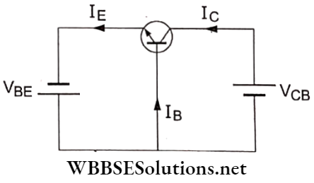
Question 28. An n-p-n transistor conducts when
- The collector is positive and at the same potential as the base
- Both the collector and the emitter are negative with respect to the base
- Both the collector and the emitter are positive with respect to the base
- The collector is positive and the emitter is negative with respect to the base
Answer: 4. The collector is positive and the emitter is negative with respect to the base
In a transistor, the input side (base-emitter junction) is forward-biased and the output side (collector-base junction) must be reverse-biased. Hence, for an. n-p-n transistor, the collector is positive and the emitter is negative, as shown in the adjoining diagram.
Question 29. One way in which the operation of an n-p-n transistor differs from that of a p-n-p transistor is
- The emitter junction injects minority carriers into the base region of the p-n-p transistor
- The emitter injects holes into the base of the p-n-p transistor and electrons into the base region of the n-p-n transistor
- The emitter injects holes into the base of the n-p-n transistor
- The emitter junction is reverse-biased in the n-p-n transistor
Answer: 2. The emitter injects holes into the base of the p-n-p transistor and electrons into the base region of the n-p-n transistor
The emitter of a p-n-p transistor injects holes (majority carriers) into the base, whereas in an n-p-n transistor, the emitter injects electrons (majority carriers) into the base region.
Question 30. The input resistance of a silicon transistor is 100 Ω. The base current is changed by 40 μA, which results in a change in the collector current by 2 mA. This transistor is used as a common-emitter amplifier with a load resistance of 4 kΩ. The voltage gain of the amplifier is
- 4000
- 1000
- 2000
- 3000
Answer: 3. 2000
Given that input resistance =Ri=100 Ω, output load resistance = Ro = 4000Ω, change in the base current = ΔIB = 40 μA, and the corresponding change in the collector current = ΔIc — 2 mA.
voltage gain = \(A_{\mathrm{v}}=\frac{\Delta V_{\mathrm{o}}}{\Delta V_{\mathrm{i}}}=\left(\frac{R_{\mathrm{o}}}{R_{\mathrm{i}}}\right)\left(\frac{\Delta I_{\mathrm{C}}}{\Delta I_{\mathrm{B}}}\right)\)
∴ \(\left(\frac{4000 \Omega}{100 \Omega}\right)\left(\frac{2 \times 10^{-3} \mathrm{~A}}{40 \times 10^{-6} \mathrm{~A}}\right)=2000\)
Question 31. For a transistor to be active,
- The base, emitter, and collector regions should have similar sizes and doping concentrations
- The base region must be very thin and lightly doped
- The emitter-base junction is forward-biased and the base-collector junction is reverse-biased
- Both the emitter-base junction and the base-collector junction are forward-biased
Which one of the following pairs of statements is correct?
- (2) and (3)
- (3) and (4)
- (4) and (1)
- (1) and (2)
Answer: 1. (2) and (3)
The middle layer (base) in a transistor is very thin and very lightly doped. The emitter-base junction is always forward-biased, whereas the collector-base junction is reverse-biased.
Question 32. The given transistor operates in the saturation region. Find the value of VBB. (Given that Ro = 200 Q, Ri = 100 kΩ, VCC=3V, VBE = 0.7 VCC = 0 and β = 200.)
- 7.5 V
- 8.2 V
- 4.2 V
- 6.6 V
Answer: 2. 8.2 V
The voltage between the collector and the emitter is
⇒ \(V_{\mathrm{CE}}=V_{\mathrm{CC}}-I_{\mathrm{C}} R_{\mathrm{o}}=0 \text { (given) }\)
∴ \(3 \mathrm{~V}=I_{\mathrm{C}}(200 \Omega) \Rightarrow I_{\mathrm{C}}=\frac{3}{200} \mathrm{~A}=15 \mathrm{~mA}\)
∵ \(\beta=\frac{I_{\mathrm{C}}}{I_{\mathrm{B}}}=200 \text { (given) }\),
∴ base current = \(I_{\mathrm{B}}=\frac{I_{\mathrm{C}}}{200}=\frac{15 \mathrm{~mA}}{200}=0.075 \mathrm{~mA}=75 \mu \mathrm{A}\)
For the closed loop containing the base and the emitter,
⇒ \(V_{\mathrm{BE}}=V_{\mathrm{BB}}-I_{\mathrm{B}} R_{\mathrm{i}}\)
⇒ \(V_{\mathrm{BB}}=0.7 \mathrm{~V}+(75 \mu \mathrm{A})(100 \mathrm{k} \Omega)\)
∴ \(0.7 \mathrm{~V}+\left(75 \times 10^{-6} \times 10^5 \mathrm{~V}\right)=8.2 \mathrm{~V}\)
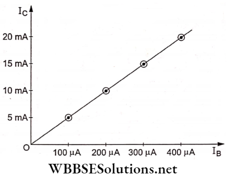
Question 33. The transfer characteristic curve of a transistor having input and output resistances of 100 Ω and 100 kΩ respectively is given in the adjoining 10 mA figure. The voltage gain and the power gain are respectively
- 5 x l04 and 2.5 x l06
- 2.5 x 10⁴ and 2.5 x 10⁶
- 3.5 x l04 and 5 x l05
- 4 x 10⁴ and 5 x 10⁶
Answer: 1. 5 x l04 and 2.5 x l06
Voltage gain = \(\frac{\text { output voltage }}{\text { input voltage }}\)
∴ \(\left(\frac{I_{\mathrm{C}}}{I_{\mathrm{B}}}\right)\left(\frac{R_{\mathrm{o}}}{R_{\mathrm{i}}}\right)=\left(\frac{5 \mathrm{~mA}}{100 \mu \mathrm{A}}\right)\left(\frac{100 \mathrm{k} \Omega}{100 \Omega}\right)\)
⇒ \(\frac{5 \times 10^{-3} \mathrm{~A}}{100 \times 10^{-6} \mathrm{~A}} \times \frac{100 \times 10^3 \Omega}{100 \Omega}=5 \times 10^4\)
∴ power gain = (voltage gain)(current gain)
⇒ \(\left(5 \times 10^4\right)\left(\frac{I_{\mathrm{C}}}{I_{\mathrm{B}}}\right)=\left(5 \times 10^4\right)\left(\frac{5 \mathrm{~mA}}{100 \mu \mathrm{A}}\right)\)
⇒ (5 x 10⁴)(50) = 2.5 x 10⁶.
Question 34. An n-p-n transistor operates as a common-emitter amplifier with a power gain of 60 dB. The input resistance is 100 Ω and the output load resistance is 10 kΩ. The current gain β is
- 3
- 60
- 102
- 6 x l02
Answer: 3. 102
Power gain = (current gain)(voltage gain)
⇒ \(\beta\left(\frac{V_{\mathrm{o}}}{V_{\mathrm{i}}}\right)=\beta\left(\frac{I_{\mathrm{o}} R_{\mathrm{o}}}{I_{\mathrm{i}} R_{\mathrm{i}}}\right)=\beta^2\left(\frac{R_{\mathrm{o}}}{R_{\mathrm{i}}}\right)\)
Given that power gain = 60 dB = 10 log \(\left(\frac{B^2 R_{\mathrm{o}}}{R_{\mathrm{i}}}\right)\)
∴ \(\frac{\beta^2 R_{\mathrm{o}}}{R_{\mathrm{i}}}=10^6 \Rightarrow \beta^2\left(\frac{10 \mathrm{k} \Omega}{100 \Omega}\right)=10^6\)
⇒ β2 =104.
∴ current gain = β =100
Question 35. An n-p-n transistor is used in the common-emitter configuration as an amplifier with a load resistance of 1 kΩ. A signal voltage of 10 mV is applied across the base-emitter junction. This produces a 3 mA change in the collector current and a 15 μA change in the base current of the amplifier. The input resistance and the voltage gain are respectively
- 0.33 kΩ and 300
- 0.67 kΩ and 300
- 0.33 kΩ and 1.5
- 0.67 kΩ and 200
Answer: 2. 0.67 kΩ and 300
Given that RC=1 kΩ =1000 Ω, input voltage = Vi =10 mV, change in the collector current = ΔIc = 3 mA, and ΔIB =15 μA.
is transistor in neet syllabus 2023
∴ input resistance = \(R_{\mathrm{i}}=R_{\mathrm{BE}}=\frac{\Delta V_{\mathrm{i}}}{\Delta I_{\mathrm{B}}}=\frac{10 \mathrm{mV}}{15 \mu \mathrm{A}}=\frac{2}{3} \times 10^3 \Omega\)
∴ voltage gain = \(\frac{V_{\mathrm{o}}}{V_{\mathrm{i}}}=\frac{\Delta I_{\mathrm{C}} R_{\mathrm{C}}}{\Delta I_{\mathrm{B}} R_{\mathrm{i}}}=\frac{\left(3 \times 10^{-3} \mathrm{~A}\right)(1000 \Omega)}{\left(15 \times 10^{-6} \mathrm{~A}\right)\left(\frac{2}{3} \times 10^3 \Omega\right)}=300\)
Question 36. In the given diagram, the supply voltage (VBB) can vary from zero to 5.0 V, VCC = 5 V, βDC = 200, and VBE =1.0 V. The minimum base current and the input voltage at which the transistor will go to saturation are respectively
- 25 μA and 2.8 V
- 2.0 μA and 2.8 V
- 25 μA and 3.5 V
- 20 μA and 3.5 V
Answer: 3. 25 μA and 3.5 V
In a transistor, saturation occurs when VCE = 0.
Applying the loop rule in the given loop, we have
VCE – VCC + ICRC = 0
⇒ VCE = 0 = VCC – ICRC
⇒ \(I_{\mathrm{C}}=\frac{V_{\mathrm{CC}}}{R_{\mathrm{C}}}=\frac{5 \mathrm{~V}}{1 \mathrm{k} \Omega}=5 \times 10^{-3} \mathrm{~A}\)
∴ \(\beta_{\mathrm{DC}}=\frac{I_{\mathrm{C}}}{I_{\mathrm{B}}}=200 \text { (given) }\)
∴ base current = \(I_{\mathrm{B}}=\frac{I_{\mathrm{C}}}{200}=\frac{5 \times 10^{-3} \mathrm{~A}}{200}=25 \mu \mathrm{A}\)
Again applying the loop rule for the base-emitter closed loop, we obtain
VBE – VBB + IBRB= 0
⇒ VBB = (25 x 10-6 A)(100 x103 Ω) +1 V
= 3.5 V.
Question 37. A common-emitter amplifier circuit built using an n-p-n transistor is shown in the figure. Its DC current gain is 250, Rc =1, and VCC = 10V. What is the minimum base current for VCC to reach saturation?
- 10μA
- 100 μA
- 40 μA
- 7 μA
Answer: 3. 40 μA
Given that DC current gain = \(\frac{I_{\mathrm{C}}}{I_{\mathrm{B}}}=250, R_{\mathrm{C}}=1 \mathrm{k} \Omega \text { and } V_{\mathrm{CC}}=10 \mathrm{~V}\)
For saturation, VCE = 0.
Thus, VCC = ICRC
is transistor in neet syllabus 2023
⇒ \(I_{\mathrm{C}}=\frac{V_{\mathrm{CC}}}{R_{\mathrm{C}}}=\frac{10 \mathrm{~V}}{1 \times 10^3 \Omega}=1 \times 10^{-2} \mathrm{~A}\)
Now, \(\frac{I_{\mathrm{C}}}{I_{\mathrm{B}}}=250\)
∴ base current = \(I_{\mathrm{B}}=\frac{I_{\mathrm{C}}}{250}=\frac{10^{-2} \mathrm{~A}}{250}=40 \mu \mathrm{A}\)