WBCHSE Class 12 Physics Communication System Notes

WBCHSE Class 12 Physics Notes

Communication System Introduction

The term ‘communication’ has a broad and pervasive significance in our everyday lives, particularly due to the advancements in modern technology. Communication refers to the conveyance of information or ideas by many channels such as verbal and non-verbal language, written materials like books and magazines, electronic media like radio, television, and video, as well as modern technologies like mobile phones, telephones, and the internet. The significance of the communication system, as seen above, cannot be overstated. In any communication system, there are two distinct points known as the transmitter and the receiver. The content conveyed is sometimes referred to as a message, data, or information. Any form of communication, whether it is audio-visual or sent through any medium, is considered a message or data in its own right.

The communication system can be classified into three categories:

Read and Learn More Class 12 Physics Notes

One-way communication 

Here the transmitter only communicates message or information to the receiver, but the receiver, in exchange, cannot communicate anything

Communication System One Way Of Comminication

Example: Books, music, radio, and TV one-way intercom are examples of this kind

Both-way or full-duplex or interactive communication

In this type of communication, the receiver receives information from the sender, and at the same time, it communi¬ cates counter-message or information to the sender. In this way-there goes on a mutual message-transfer transmitted between the sender and the receiver.

Communication System Interactive Comminication

WBCHSE class 12 physics notes Half-duplex communication

In between these two categories, there is a system where there is a scope of exchanging me$sage£both ways, but which never happens at the same time

Example: SMS or e-mail, through which only after the completion of sending a message from one end, the counter-message can be communicated from the other end. There is no scope for simultaneous message transfer between the sender and the receiver

Timetable of communication system:

Communication System Time Table Of Communication System

WBBSE Class 12 Communication System Notes

In this chapter, we will concern ourselves with distant communication. For communication, within our audible and visible range, no technology is necessary. On the other hand, by applying electromagnetic waves through various technological processes, distant communication has made an incredible development in the last 20/30 years. A list of development of communication science

WBCHSE class 12 physics notes 

Elements Of Communication System.

Message signal or data signal:

  • The data or message to be transmitted is converted into a similar electrical wave at the transmitter end. As an audio wave is converted into a similar electrical wave by a microphone.
  • The next step is to transmit this electrical wave through a transmitting antenna, as a similar electromagnetic wave (i.e., as a message signal or data signal) to distant places.
  • In reality, however, the direct transmission of this data signal is practically impossible. Hence, the help of electromagnetic carrier waves is taken.

Carrier wave and transmission band:

Carrier waves are used for carrying the data signal effectively from the transmitter end to the receiver end. The frequency of the carrier wave is much higher than the frequency ofthe data signal i.e., its wavelength is small.

Thus the antennas of transmitters and receivers can function properly. Moreover, the distortion created by the superposition of different data signals at the receiver end is eliminated. Electromagnetic waves of any frequency chosen from a wide range of frequencies can be used as a carrier wave.

But first, the main objective of transmission has to be determined. Then the frequency of the carrier wave is chosen accordingly. For example, for radio transmission up to 200 km, a medium wave (with frequency ≈ 3 × 10⁶ Hz-3 × 10⁶ Hz ) would be adequate. For a particular transmission, the range of frequency used is called the transmission band.

Communication System Class 12 Notes

Communication medium or transmission medium:

To reach the receiver end, the carrier wave essentially requires a medium. A medium is selected in such a way that the wave pattern of data signal is received in an undistorted condition.

Generally the media used are:

  1. Atmosphere for wireless communication
  2. Coaxial cable and
  3. O(ptical fiber for wired communication.

Communication channel:

Th transmission medium and the transmission band together form a communication chanel.

‘A short wave is being transmitted through the atmosphere statement indicates a particular communication channel with frequencies between 3 × 10⁶ Hz-3 × 10⁶ Hz. Different zones of atmosphere are chosen for the transmission of different frequencies. The technological means to be adopted for this are also predetermined. Hence, in communication science, the concept of communication channel is of paramount importance

WBCHSE Class 12 Physics Communication System Notes

Terminologies used in communication system

Modulation:

As the frequency of the original message or data signal is very low, it cannot travel a very long distance on its own. So, for transmitting it through a long distance, it is super¬ imposed on a high-frequency carrier wÿve. The process of imposing data signal on a carrier wave of specific amplitude and frequency is called modulation. Some important modulations are >0 Amplitude Modulation .. (AM),0 Frequency Modulation (FM), and Phase Modulation (PM).

Demodulation:

The modulated wave being transmitted from the transmitter end is collected at the receiver end. Once again the data signal is separated from the wave. This is called demodulation. Arrangements are made to convert the separated data signal 1 again into the original message or data. As, to con¬ vert demodulated audio signal into sound, the loudspeaker is used.

Communication System Class 12 Notes 

Noise:

Noise refers to the disruption or alteration of the original waveform of the transmitted signal. However, in reality, when a signal is transferred from the transmitting station to the receiving station, or from an intermediate receiving station to the next receiving station in increments, some interference is introduced into the original signal at each step. Consequently, the data that is received cannot be identical to the data that was transmitted. It is possible to distinguish the speaker’s original voice from the sound produced by the speakers.

Short Notes on Modulation Techniques

Generally, the noise is classified into two categories:

  1. Controllable noise: Defects in the equipment or their components give rise to this type of ‘noise which can be largely eliminated by using improved instruments. Hence, this defect is most often not treated as noise at all. Obviously, by using high-quality loudspeakers, the degree of noise can be reduced substantially.
  2. Random noise: These noises are not at all within our control. Hence these types of noises can never be eliminated

Block diagram of a communication system

In the main components of a standard communication system is shown in the form of a block diagram

Communication System Black Diagram Of Communication System

Community System Types Of Transmission Data

In distant communication, the transmitted data or messages are basically of three types. Those are described below.

Audio data

Transmissible dialogue or any other sound can be referred to as audio data. Every piece of information is produced as a sound wave with a frequency ranging from 20 Hz to 20,000 Hz, also known as Audio Frequency (AF). The complete spectrum of frequencies within this range is referred to as the auditory frequency range. Using a microphone or similar setups, these sound waves are transformed into corresponding alternating voltages.

In order to convey it to the receiving location, a transmitting antenna is utilized to emit the alternating voltage as electromagnetic waves. In order for the electromagnetic waves to accurately represent the original sound, it is necessary for the frequency of the original sound wave and the electromagnetic wave to be identical.

The changes in the amplitude of these two waves also have to be identical. This electromagnetic wave Is the audio signal. As the audio message is a sound wave, its speed in the air at 20°C is approximately 330 m. s-1 . But the audio signal is an electromagnetic wave, its speed in air is 3 × 10⁸ m. s-1

Let the frequency of an audio message be 3 kHz. As the frequency of the generated audio signal has to be the same, the wavelength of the signal is

λ = \(\frac{\text { velocity }}{\text { frequency }}\)

= \(\frac{3 \times 10^8 \mathrm{~m} \cdot \mathrm{s}^{-1}}{3 \times 10^3 \mathrm{~s}^{-1}}\)

= 105 m

= 100 km

To transmit this signal directly through a transmitting antenna an antenna of the same size as the wavelength is required, which is practically impossible. For this reason, no audio signal can be transmitted directly from the transmitter end to the receiver end. This constraint applies not only to audio signal but to the following two messages (data) signals also

Important Definitions in Communication Systems

Audio-Visual or video data

Video data refers to any form of visual content, including pictures, handwritten or printed documents, still or video images, that is transmitted electronically. Audio data is overlaid upon video data in television and other comparable transmissions, resulting in what is known as audio-visual data. However, in general, the phrase ‘video data’ encompasses the combination of both audio and visual data.

A microphone is employed to transform audio data into an audio signal, while a camera scanner serves the same purpose for video data by turning it into video signals. This camera utilises a specialised method to scan an image and simultaneously produces corresponding electromagnetic video signals that accurately represent the brightness and colour of the image.

Digital data

Digital data comprises a sequence of lay¬ ers of low and high potentials, where the magnitudes of the potentials are not Important. Bather, the duration of the alternat¬ ing voltages in different layers plays the decisive part In digital transmission, the original audio and visual data are not converted into analogue alternating voltage.

With the advancement of digital electronics, today many types of data, including computer data, are generated as digital data. By applying a special process to this digital data, electromagnetic digital signals are generated. In practice, however, no data signal Is suitable for direct distant communication.

Communication System Digital Data

There are two reasons for this:

  1. From a technical point of view, it needs a huge-sized transmitter and receiver antenna and that is impossible to manufacture.
  2. Voluminous transmitted data from many transmitting cenÿ could crowd the receiving station % at the & same time. Their superposition may generate a fuzzy and unrecognizable signal.

If the data signal contains a single frequency, then the waveform is sinusoidal. But in reality, no waveform of a signal is purely sinusoidal. Hence whatever form it may have, it is treated as a wave generated from the superposition of many sinusoidal waves.

Communication System – Carrier Wave

The carrier wave is employed to mitigate the aforementioned challenges in long-distance transmission of data streams. The term “wave” is used to describe the transmission of the data signal from the transmitter to the receiver. Carrier waves are characterised by a significantly greater frequency compared to any data transmission.

Put simply, its wavelength is far smaller than that of data signals. It is important to note that the frequency range of the audio signal, which serves as the data signal, spans from 20 Hz to 20 kHz. This range is commonly referred to as the Audio Frequency range or AF range.

Every carrier wave is an electromagnetic wave. Typically, carrier waves in the electromagnetic spectrum consist of waves with lower frequencies. Typically, electromagnetic waves in the frequency range of 3 kHz to 300 GHz consist of radio waves and microwaves. In the realm of communication, the utilisation of the remaining portion of the spectrum is virtually nonexistent. The carrier waves are categorised into many groups based on their distinct objectives and applications in long-distance communication.

Communication System Carrier Wave

When a data signal is to be transmitted from one place to another, the suitable carrier wave is selected at the very beginning. From the table, it is clear that the frequency which is suitable for radio transmission is not suitable for TV transmission

Communication System Class 12 Notes Bandwidth

An ideal carrier wave is a purely sinusoidal electromagnetic wave with a definite frequency. However, any attempt to generate a wave invariably results in the main frequency being superimposed with several other higher or lower frequencies. The intensity of the carrier wave is maximum for only its main frequency f0. However, the intensities of other frequencies on either side of f0 diminish gradually

Communication System Band Width

Suppose that the intensity of each of the frequencies f1 and f2 on either side of f is half of the maximum intensity, which means that the rate of energy or power carried is also equal to half of the maximum value. These two frequencies a f1nd f2 are called half-power frequency.

Only when the frequency gets lower than f1 or higher than f2, the intensity of the wave becomes negligible. So, though the main frequency of the carrier wave is f0, the intensity or amount of energy carried by the waves between the frequencies f1 and f2 cannot be ignored. This difference of frequencies (f2-,f1) is called the bandwidth of the carrier wave. As data signal is superimposed on carrier waves, it is also called signal bandwidth.

As a frequency-intensity graph becomes sharper, the bandwidth gets reduced. Hence the problem due to the mixing of different carrier waves is also reduced. As per international norms for radio transmission, it is desirable that the band¬ width should not exceed 5 Hz, and the difference between two main frequencies (JQ) of carrier waves, transmitted from two transmitting stations, should be at least 10 kHz.

Each carrier wave of every transmitting station carries its own data signal. The carrier waves are recognized at the receiving stations, only due to the difference of their frequencies. Hence the data signals do not become fuzzy or unrecognisable by intermixing i.e., remain distinct from each other.

Class 11 Physics Class 12 Maths Class 11 Chemistry
NEET Foundation Class 12 Physics NEET Physics

Communication System – Modulation And Demodulation

It has been mentioned that the process of superimposing the low-frequency data signal on a high-frequency carrier wave at the transmitting end is called modulation. On the other hand, the process of separating the superimposed data signal from the carrier wave at the receiving end is called demodulation.

Let the equation of carrier wave be,

V= V0 sin(Ωt + θ)

[Where, V0 = amplitude of the wave, Ω = Angular frequency, Ωt + θ = phase of the wave = Φ(say), θ = initial phase or epoch

Linear frequency or simply the wave frequency

n =  \(\frac{\Omega}{2 \pi}, \text { where } \Omega=\frac{d \phi}{d t}\)

For convenience, the initial phase 6 can be taken as zero.

In that case,

The carrier wave: V = V0 sin Ω t ……………………………………… (1)

Similarly, the equation of the data signal,

v0 = v0  sinωt  ………………………………………… (2)

[where, v0 = amplitude of the wave and co = angular frequency]

The instantaneous voltage v is called the modulating voltage

The condition of effective modulation of the carrier wave of equation (1) by modulating the data signal of equation (2) is,

ω<<Ω

The frequency of the carrier wave should be much higher than the frequency of the data signal. In practice, this frequency is 1000 times or even more than that of the data signal. The modulating voltage generally fluctuates very slowly with time and hence the wave indicating data signal is frequently called slow wave.

Class 12 Physics Communication System

Amplitude Modulation (Am) And Amplitude Demodulation

Amplitude Modulation or AM Definition:

In the case of distant communication, after the imposition of a data signal on a carrier wave, if the frequency remains unchanged and only the amplitude changes in a slow, periodic way, then the process is called Amplitude Modulation or AM.

Let, on the carrier wave of equation (1)  the data signal of equation (2) be superimposed in such a way, that the value of amplitude V0 changes with time. With the stationary value of amplitude V0 of the carrier wave, a sinusoidal alternating voltage kv0 sincot gets added, i.e.,

Vm0(t) = V0 +kv0sinωt ……………………… (1)

Where k is a dimensionless constant. Vm0 is the amplitude of generated modulated voltage due to modulation of a carrier wave by data signal.

As ω<<Ω, so the change of voltage is very slow.

Modulated voltage, Vm = Vm0 sinΩt

= (V0 +kv0 sinωt )sin Ωt

∴ V= V0 (1+β+sin ωt ) ……………………..(2)

Where β = \(k \frac{v_0}{V_0}[/atex] = modulation index

The significance of equation (2):

  1. The existence of sinΩt indicates that, due to modulation, the frequency of carrier wave (Ω) does not change with time.
  2. sin ωt can be both negative and positive. As the value of co is very low, the multiplier (1 + βsinωt) of the amplitude V0 indicates that the amplitude of the modulated wave fluctuates very slowly on either side of V0.

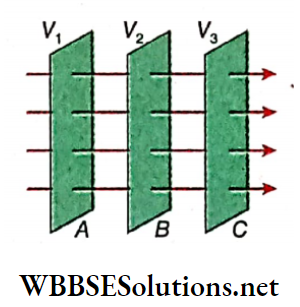
The carrier wave is shown as a sinusoidal curve of a particular frequency and also a data signal is shown as a sinusoidal curve of another particular frequency. In both cases, with the two waves, their corresponding alternating sine voltages are taken as the vertical axis

Communication System Alternating Sine Voltages As The Vertical Axis

Communication System Alternating Sine Voltages As The Vertical Axis.

A carrier wave, when modulated by a data signal, is the nature of the AM wave thus produced.

Communication System Modulated By A Data Signal

Sideband

From equation (2),

V = V0 sin Ωt +βV0 sinΩt sin ωt

= V0 sin Ωt + [latex]\frac{\beta V_0}{2}\) cos (Ω – ω)t – \(\frac{\beta V_0}{2}\) cos (Ω + ω)t ……………… (3)

Equation (3) reveals that AM wave consists of sinusoidal components of three frequencies Ω, Ω- ω, and Ω+ ω. Though the frequency of the carrier wave does not change with time, the other two frequencies overlap with the main frequency f (both cosine and sine functions are sinusoidal).

In this discussion, the data signal has been taken as composed of a single frequency co. In audio signal, can be considered to be a signal generated from a pure tone, and in video signal, is a monochromatic signal. In most practical cases, however, quite a of sinusoidal frequencies lie superimposed on the original data signal.

Let us suppose, in a data signal, frequencies of range ω to ω ±Δω are mixed up. In that case, if the (ω → ω ±Δω) range is considered in place of co in equation (3), then the frequencies present in the amplitude-modulated wave are

Ω: Point O

The frequencies of (Ω + ω) to (fl + (Ω + ω +Δω ) range:

Part BD

The frequencies of(Ω – ω – Δω) to (Ω – ω ) range:

Part CA

Communication System Sideband Of Range

Here, the frequency range CA and BD are called the sidebands of the amplitude-modulated wave. The maximum and minimum frequencies of the full wave are (Ω + ω +Δω) (point D) and (Ω – ω -Δω) (point C). The CD stretch of the frequency is called the bandwidth of the AM wave. The magnitude of the bandwidth is,

d = CD = (Ω + ω +Δω)- (Ω – ω -Δω) = 2(ω + Δω)

= 2 × maximum frequency on the data signal

To transmit the AM wave properly, a communication channel is to be selected, the transmission band of which should be extended at least from (Ω + ω +Δω) to (Ω – ω -Δω) i.e., from point C to D . However, instead of both the sidebands, transmission by using only one sideband is also in practice. In that case, transmission can be done with half bandwidth. This is called single-sideband communication.

Demodulotion principle of AM wave

A well-selected circuit performs the function of amplitude modulation. Now the modulated wave is applied to a transmitting antenna. The waveform of the electromagnetic wave thus generated and spread all over is exactly similar to the modulated waveform.

Transmitted through the communication medium, the electromagnetic wave reaches the receiving antenna (one or more than one), and in each antenna, an exactly similar potential wave is generated from the electromagnetic wave. Naturally, the intensity of the wave at the receiving end is much less than that at the transmitting end.

In the next step, keeping the waveform intact, the intensity ofthe wave is multiplied several times by using a suitable amplifier. Then, with suitably selected circuitry, the carrier wave and the data signal are separated from the mixed wave. This is the process of demodulation its other popular name is detection. Demodulation of the amplitude-modulated wave is also called Peak Detection.

Radio receiver:

At last, the demodulated data signal is amplified again, and with the right procedure(as in audio signal, through loudspeaker) the data generated from the transmitting end, is traced. In audio signal, the entire machinery set up is called a radio receiver.

Communication System Radio Receiver

It can be mentioned here that, the process of demodulation of frequency-modulated wave Is also exactly similar to this though the circuitry Is different.

Production of an AM wave

An n-p-n transistor T. At the very beginning, a dc circuit of the transistor Is constructed by using the necessary bias voltage and different resistances. An operating point Is also fixed. These dc components of the circuit have not been

Communication System Production Of An AM Wave

Now by using the appropriate DC filter, the alternating voltage of the carrier wave is applied to base B of the transistor, and the alternating voltage of the data signal is applied to collector C. Depending on the fluctuation of the voltage of the data signal, the collector current changes and thus, at output of transistor, an identical replica of data signal gets mixed on the amplified carrier wave and an amplitude modulated wave is generated. Necessary filter arrangements are made so that no DC component of the current can mix with it.

Amplitude modulators are basically of two types:

  1. Linear modulator, used in radio transmission
  2. Square-law modulator, used in a telephone conversation

Defection of an AM wave

The circuit is commonly employed as an AM wave demodulator. The device is commonly referred to as an envelope detector. The circuit consists of a semiconductor diode D, which is specifically designed to function as a half-wave rectifier, together with an RC filter.

At the peak of the positive half cycle of the carrier wave in an AM wave, the capacitor C reaches its maximum charge. As the carrier voltage lowers gradually, the charge of capacitor C diminishes due to dissipation through resistor R.

The time constant of the RC circuit, denoted as CR, is set to a value somewhat larger than the duration of the carrier wave and slightly smaller than the period of the data signal. Consequently, the charge of C does not exhibit the same rate of increase or drop as the phases of a carrier wave. Instead, the waveform of the data stream is represented by the fluctuation in the charge of capacitor C.

At output, the waveform of the carrier is not available, the output wave mainly indicates the waveform of the data signal. This envelope detector is a linear detector, because, here the output voltage becomes proportional to the input voltage. To ensure that no component of DC can pass to output, capacitor C’ is used as a filter in the circuit, as

Communication System Detection Of An AM Wave

Frequency Modulation And frequency Demodulation

Frequency Modulation Definition:

In distant communication, after superimposing a data signal on a carrier wave, if the amplitude remains unchanged and only the frequency changes in a slow periodic way, then the phenomenon is called Frequency Modulation or FM.

Equation of carrier wave,

V = V0sinΩt = V sin Φ ………………………………….. (1)

Where phase angle, Φ = Ωt

i.e  \(\frac{d \phi}{d t}=\Omega\)  = Ω …………………………………. (2)

And, The equation of data signal

v = v0 sincωt …………………………………. (3)

Keeping the amplitude V0 of the carrier wave unchanged, the time-dependent data signal is superimposed on it.

Due to modulation, the instantaneous value of frequency Ω is,

Ωm (t) = Ω + kv0 sinωt …………………………………. (4)

Here, k is a coupling constant that converts v0 sinωt into a frequency-dependent term.

In this case, the unit of k will be V-1. s-1

( kv0 sinωt) will be s-1 , i.e., Hz. Applying equation (2) for this time-dependent frequency we get,

m =  Ωm (t)dt

Or, Φm = ∫ Ωm (t)dt= Ω ∫ dt + kv0 ∫ sinωt dt

Or, Φm = Ωt – \(\frac{k v_0}{\omega} \cos \omega t+\delta\) cosωt + δ …………………………. (5)

Writing time-dependent phase angle Φm in place of Φ in equation (1) of carrier wave we get

Vm = V sin ( Ωt – β cosωt + δ) …………………………… (6)

Where,  β = \(\frac{k v_0}{\omega}\)

This is the equation of frequency modulated wave or FM wave. In this equation

β = \(\frac{k v_0}{\omega}\)

In this case:

The amplitude V0 of the carrier wave does not change.

For the term (β cosωt), the frequency of carrier wave fluctuates with time.

As ω<<Ω, this change of frequency is slow. This phenomenon is called frequency modulation.

A carrier wave, a data signal, and a form of FM wave, generated due to the superimposition of these two waves, are shown respectively.

Communication System Frequency Modulation And Frequency Demodulation

It is observed that in the AM wave, besides the frequency Ω of the carrier wave, two more sine components of frequencies (Ω – ω) and (Ω + ω) are present. But on mathematical analysis of frequency modulated wave, it is found that the number of sine components is infinite. The frequency of the components are Ω ±ω, Ω ±2ω, Ω ±3ω, ………………. etc.

These frequencies lie symmetrically on either side of the frequency of the carrier wave Ω.

In transmission through Low Frequency (LF) or Medium Frequency (MF) carrier wave, amplitude modulation is generally employed while in transmission through High Frequency (HF) or Very High Frequency (VHF) carrier wave, frequency modula¬ tion is employed. The range of frequencies of HF or VHF is very high, so the differences in frequency of the carrier waves, transmitted from different transmitting centers, are also very high.

Hence, despite the presence of sideband frequencies in FM waves, the possibility of overlapping of different waves and noise and distortion of data signal due to this becomes very low. For this reason, the sound of FM radio is very clear and in TV, the chance of mixing pictures transmitted from two stations is almost nil.

Demodulation principle of FM wave

Typically, the recipient produces a frequency-modulated waveform, and the gradual variation in amplitude is linked to the gradual variation in frequency. The wave is subsequently applied to an appropriate detector circuit and, using a similar manner to demodulating amplitude-modulated waves, the data signal is extracted.

Currently, the superheterodyne receiver is widely used in the demodulation of FM waves. An oscillator is housed within the receiver, where it combines a wave of carefully chosen frequency with the FM wave. The procedure is quite beneficial for accurately identifying the frequency of the data signal.

Communication system physics notes Power Dissipated due to Modulation

If the potential difference across the two ends of a transmitting antenna is time-dependent and the potential difference is expressed as V(t), then the dissipated power of the antenna is

P = \(\frac{\overline{V^2(t)}}{R}\) ………………………….(1)

Here, the symbol \(\overline{V^2(t)}\) indicates the mean of the quantity Vt concerning time. R is the effective resistance of the antenna. In the case of of time-dependent voltage, due to the metallic elements of the antenna and electromagnetic radiation from it, the effective resistance R is not equal to the DC resistance of the antenna

Now, according to equation (1)

Carrier wave: V = V0 sin Ωt …………………………. (2)

Again, from equation (2), we get,

AM wave: VAM = V0(1 + β sinωt)sinΩt ………………………….. (3)

Similarly from equation (6) we get
,
FM wave: VFM = V0sin(Ωt – β cosωt) ……………………………. (4)

In both equations (3) and (4), the term is modulation index which is sometimes expressed by the symbol ‘m’ also. Each of V, VAM, and VFM indicated by the above three equations is time time-dependent potential difference. Hence, in each case, the power dissipated in the antenna is to be evaluated by using equation (1)

The power dissipated In the transmission of carrier wave:

From equation (’2)

V2 = V02 sin2 Ωt

= \(\overline{V^2}=V_0^2 \overline{\sin ^2 \Omega t}\)

We know that functions like sin Ωt If or cos Ωt are time-dependent sinusoidal functions, lit each complete cycle, the average of sin²-function or cos²-function is zero, but the average ol sin or cos-function is ½.

∴ \(\overline{\sin ^2 \Omega t}\)  = ½

Hence, the power dissipated hr antenna for transmitting carrier wave only:

PC = \(\frac{\overline{V^2}}{R}=\frac{V_0^2 \cdot \frac{1}{2}}{R}=\frac{V_0^2}{2 R}\)  ……………………………… (5)

The power dissipated In the transmission of amplitude-modulated wave:

From equation (3) we get,

AM =  V²0( 1+β sinωt)² sin²Ωt

= V²0( 1+2β sinωt +β² sin² ωt)  sin²Ωt

So,  \(\overline{V_{A M}^2}=V_0^2\left(1+2 \beta \overline{\sin \omega t}+\beta^2 \overline{\sin ^2 \omega t}\right) \overline{\sin ^2 \Omega t}\)

= (1+ 2β.0+β .½). .½ = \(\frac{V_0^2}{2}\left(1+\frac{\beta^2}{2}\right)\)

Hence power dissipated in the antenna,

PAM =  \(\overline{\frac{V_{A M}^2}{R}}=\frac{V_0^2}{2 R}\left(1+\frac{\beta^2}{2}\right)\)

Or, PAM =  \(P_C\left(1+\frac{\beta^2}{2}\right)\) ……………………………………… (6)

The significance of this equation is that the power dissipated in the antenna increases in transmitting amplitude modulated wave compared to that in transmitting only the carrier wave. The amount of increase is

P’= PAM – PC = \(P_C\left(1+\frac{\beta^2}{2}\right)-P_C=P_C \cdot \frac{\beta^2}{2}\)  ……………………………… (7)

i.e., the rate of dissipation of additional power or energy is proportional to the square of the modulation index. As, for 100% modulation, β = 100% = 1

So, PAM =   \(P_C\left(1+\frac{1^2}{2}\right)\) = \(\frac{3}{2}\) PC

In this case Increase In dissipated power

P’ = \(\frac{3}{2}\) PC  – PC = \(\frac{1}{2}\) PC

i. e amount of Increase Is 50%.

It may the noted that dial tho additional dissipated power duo to amplitude modulation Is equally divided between die two side hands. I,e„ dissipated power for each sideband

= \(\frac{p^{\prime}}{2}\)

= PC. \(\cdot \frac{\beta^2}{4}\)

Communication System Physics Notes

The power dissipated In the transmission of frequency-modulated wave:

Prom equation (4),

⇒ \(v_{l M}^2=v_0^2 \sin ^2(\Omega-\beta \cos \omega t)=V_0^2 \sin ^2 \phi_{l_M}\)

Where ΦFM = Ωt – β cosωtCommunication system physics notes

So, \(\overline{v_{P M}^2}=v_0^2 \overline{\sin ^2 \phi_{I M}}=v_0^2 \cdot \frac{1}{2}\)‘

Hence, energy dissipated in the antenna

PFM = \(\frac{\overline{V_{I M}^2}}{R}=\frac{V_0^2}{2 R}\)  = PC ……………………….. (8)

The significance of this equation Is that, the power dissipated in the antenna remains unchanged In transmitting frequency-modulated waves compared to that In transmitting only the carrier wave. That is, for frequency modulation, there is no change in dissipated power. This power is not at all dependent on the modulation Index, β.

Modulator-Demodulator or Modem

It is a device that converts digital data to analog data and analog data to digital data. Modern computers function on a digital scale. All the data available from it is digital. In a localized area (as in an office), where the local area network or LAN is formed by connecting the computers of the office, direct exchange of digital data takes place. In such cases, the data need not be converted to analog data, hence there is no need to use the modem. In this type of direct exchange of digital data, mainly coaxial cable is used as the medium.

On the other hand, in distant communication, the computer is connected to a telephone line through a modem. The digital data of the computer is converted into amplitude-modulated or frequency-modulated analog data by a modem. Then this analogue data reaches the computers of the worldwide network through the telephone system. The modern connection with the receiving computer on its part separates the primary digital from the modulated analog data.

Communication System – Propagation Of Carriers Waves Through Atmosphere

When electromagnetic carrier waves of range from Very Low Frequency (VLF) to microwave (as stated in table 1) propagate through the atmosphere.

Mainly three types of waves are produced

  1. Ground wave
  2. Space wave
  3. Skywave

Suitable waves for transmission and its corresponding range of frequency of carrier wave are to be selected first and their technological set-ups are to be arranged accordingly.

1. Ground wave: This wave propagates from one point to another, along the surface of the earth following the earth’s curvature. For the propagation of this wave, the earth’s surface at one side and the lowest layer of the ionosphere (which is nearly 80 km above the earth’s surface) at the other both act as reflectors. The wave progresses through successive reflections which it suffers from these two surfaces.

Communication System Ground Wave Transmitting Antenna

Another special feature of the wave is the polarisation of the transmitting antenna is placed vertically, so the wave gets polarised at a vertical plane at the start i.e., its electrical field has no horizontal component and initial wavefront is a vertical wavefront.

Now, as the wave progresses along the earth’s surface, the wavefront gradually gets tilted from the vertical line, which means that the magnitude of the horizontal component of its electrical field starts Increasing. The horizontal component of the transmitted energy gets absorbed on the earth’s surface. As the tilt of the wavefront towards the horizontal plane increases, the rate of absorption of energy continues to Increase. Therefore ground wave is not suited for long-range communication.

Communication System Tilting Of Groung Wave With The Time

Ground wave plays a very important role in transmission through carrier waves of Very low Frequency (VLF) and Low Frequency (LF). In the case of higher frequencies, the energy carried by ground waves gets absorbed very fast. This is why FM radio or television signals can be transmitted only up to a short distance.

2. Space wave:

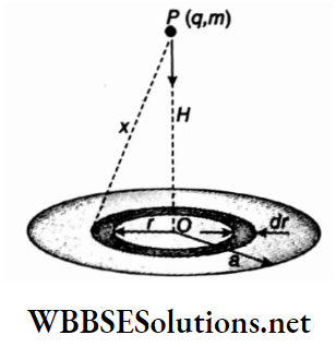
This type of wave can propagate through the atmosphere in a straight fine almost without any deviation. Due to the curvature of the earth’s surface, we can communicate through rectilinear space wave up to a distance of a certain limit. It Is called the radio horizon of the corresponding antenna

The space wave can propagate up to a maximum point O from the transmitting antenna. The distance PO of the earth’s surface is the radio horizon of the antenna.

Communication System Space Wave

Let R = radius of earth

H = Height of transmitting antenna A

From we get

cosθ = \(\frac{O C}{A C}=\frac{R}{R+H}=\frac{1}{1+\frac{H}{R}}\)

= \(\left(1+\frac{H}{R}\right)^{-1}\)

cos²θ = \(\left(1+\frac{H}{R}\right)^{-2}\) ≈ 1 – \(\frac{2 H}{R}\)

(As H<<R)

Now sin²θ  = \(\frac{2 H}{R}\)

Or, sin= \(=\sqrt{\frac{2 H}{R}}\)

As θ is very small, sin θ ≈ θ

So,  θ = \(=\sqrt{\frac{2 H}{R}}\)

Hence, radio small, horizon,

PO = Rθ

= R \(\sqrt{\frac{2 H}{R}}\)

= \(\sqrt{2 H R}\) ……………………………….. (1)

Similarly in the radio horizon of receiving antenna B, QO= \(\sqrt{2 R h}\)

When both transmitting and receiving antennas are used at the same time, the magnitude of the radio horizon is,

PQ = PO+QO = \(\sqrt{2 H R}+\sqrt{2 h R}\)

= \(\sqrt{2 R}(\sqrt{H}+\sqrt{h})\)  ………………………………………….. (2)

For example, if a space wave, transmitted from a transmitting antenna, 300 m high, is to be received by a receiving antenna 30 m high, the radio horizon will be.

= \(\sqrt{2 \times(6400 \times 1000)}(\sqrt{300}+\sqrt{30})\)

≈  81.6 ×10³ m = 81.6 km

[The radius of the earth has been taken as 6400 km ]

If carrier wave of High Frequency (HF) or of even higher frequency Is transmitted as a space wave, then a little energy is absorbed. So, despite the limitations of radio horizon, space waves are most suitable for very long-distance transmission.

In this process, the application of one or more Intermediate is most prevalent. Each intermediate antenna receives the transmitted signal and transmits the signal to the next antenna. In this way, the radio horizon can be enlarged to a great extent.

As a high-quality communication technique, wave communication Is Increasing day by day. The frequencies 8 of these microwaves arc very high, 300 MHz to 300 GHz.

These waves are transmitted mainly as space waves. For long-distance communication, instead of using a series of antennas, artificial earth satellites are employed. Space waves transmitted from earth surface after getting reflected from the artificial satellites, Let R = radius of the earth, reach distant places on the earth’s surface. This arrangement is called satellite communication

Communication system physics notes Communication system physics notes Skywave

Carrier waves in the Medium Frequency (MF) or Lower High Frequency (LHF) range are mostly transmitted as sky waves. The ionosphere, which spans from a height of BO km to around 400 km above the Earth’s surface, is crucial in sky wave propagation. The ionisation of air in the ionosphere is mostly caused by solar radiation during the day and cosmic rays of lower strength at night.

Therefore, the rate of ionisation The diurnal variation is far higher than the nocturnal variation. Within the ionosphere, the process of ionisation results in the creation of electrons and ions, which coexist with neutral molecules and atoms. The rate of ionisation is quantified by the quantity of unbound electrons. By considering the number of electrons per unit volume.

Her two factors are Important:

  1. Since solar radiation or cosmic radiation falls on the upper surface of the ionosphere first, the rate of ionization is higher in the upper surface. Depending on the difference of rate of ionization, the ionosphere Is divided into three lay upper layer, middle layer, and lower layer. The rate of ionization is maximum at the upper layer. The middle and the lower layer almost do not exist at night.
  2. With the change of Ionisation rate in air, the velocity of two magnetic waves through it also changes. As a result, the ionosphere acts as a refractive medium. I higher the ion-isolation rate in a layer, higher is the velocity of electromagnetic waves through It. That Is, the refractive index of this layer decreases. In the layers of the Ionosphere, , the rate of ionization of a higher layer A  Is maximum and Its refractive index is minimum. It can be proved that for. an incident electromagnetic wave of frequency f, the refractive index of a layer of Ionosphere

Communication System Velocity Of Electromegnetic Waves

μ = \(\left(1-\frac{81 n}{f^2}\right)^{1 / 2}\)…………………………. (3)

Where, n = electron number density of that layer of the medium. Whenever a sky wave propagates through the ionosphere, to a higher layer, it advances from a higher refractive index layer to a lower refractive index layer.

When the angle of inclination of a sky wave with respect to the vertical axis decreases significantly, it is bent away from the ionisation layer with the highest altitude and lowest refractive index, and exits the ionosphere (referred to as ray ‘a’). Conversely, if a wave with a steeper incline approaches the ionosphere from below, it will experience complete internal reflection from either layer and be redirected back to the Earth’s surface.

Put simply, the transmission of the sky wave from one place on the Earth’s surface to another is a result of reflection in the ionosphere. Since the values of f are relatively low for Medium Frequency (MF) waves, the refractive indices of the ionospheric layers are also low, as indicated by equation (3). Consequently, the sky wave is reflected even from the bottom layer of the medium. This is the reason why sky waves with frequencies of this magnitude have a rather limited range while travelling across the Earth’s surface.

In contrast, High Frequency (HF) sky waves, also known as short waves, are reflected by the top layers of the ionosphere. Therefore, the waves that bounce back can travel to faraway locations on the Earth’s surface. In this scenario, these waves are partially absorbed in the medium and lower layers, resulting in a decrease in wave intensity.

During nighttime, the absorption of light is extremely little due to the near absence of the middle and lower layers. Therefore, the signal transmitted by sky waves is more potent and distinct during nighttime. Skywave is the primary factor in radio transmission. Typically, medium wave transmission is used for short distances and short wave transmission is used for greater distances via sky waves.

Other media for the propagation of earner waves

It has already been mentioned that apart from air medium, two other media are used for communication. These are:

  1. Coaxial cable: For short-distance communication, this medium is most effective.. As, in a telephone communication system or a computer network limited to a ‘ small area, the coaxial cable is widely used.
  2. Optical fiber: Unimaginable success has been achieved in worldwide telephone communication systems by using optical fiber. Through optical fiber, it is possible to transmit electromagnetic waves in the range of almost infinite frequency, very effectively.

[The detailed discussion regarding these media is not included in the present syllabus.]

Communication System  – Communication Channel

Two factors are to be ascertained first to decide how to transmit a data signal from one place to another.

  1. Medium: Atmosphere, coaxial cable, or optical fiber are used as a medium.  Sometimes combination of different types of media is also used.
  2. Range of frequency: What part of the electromagnetic spectrum would be used as a carrier wave, is also to be trained. The corresponding range of the frequency is called the transmission band.

The arrangement for transmission of data signal from one point to another with a combination of an appropriate medium and a carrier wave of appropriate frequency is called a communication channel.

As, the carrier waves, of frequency in the range of approximately 300 kHz to 10 MHz, can propagate as sky waves through the atmosphere from one place to another. Hence it is an effective communication channel. The efficiency of a communication channel is determined by the total number| of discrete data signals that can be transmitted through it, without distortion.

A carrier wave with a frequency of 1 MHz is used to transmit an audio signal. The audio signal’s frequency naturally falls within the range of 20 Hz to 20000 Hz. The bandwidth of the amplitude-modulated wave can be calculated by multiplying the carrier wave’s amplitude by the audio signal’s frequency, resulting in a bandwidth of 40000 Hz. The band is positioned symmetrically around the primary frequency, spanning from 106 Hz to 20000 Hz on one side and from 930000 Hz to 1020000 Hz on the other side. If an audio signal is transmitted from another transmitting station using a carrier wave with a frequency of 1.05 MHz, the frequency range would be located between 1030000 Hz and 1070000 Hz.

There is a clear distinction between the previous band and the current band, and they will not blend together. As a result, the receiver can easily differentiate between the two audio streams. It is evident from this example that if the difference in frequencies between two carrier waves is more than 40 kHz, the receiving machine can accurately receive the audio signals, supposing that the bandwidth of the audio signal is 40 kHz.

Now we may examine the transmission of skywave through the atmosphere. The effective frequency propagates in a range from 100 kHz to 10 MHz. This means that the width of the transmission band is approximately 10 MHz, calculated as 107 – 105 107 Hz. In order to provide a transmission that is clear and easily distinguishable, the frequency difference between the carrier waves must be a minimum of 0.04 MHz. For instance, if we consider the difference to be 0.05 MHz, then within the 10 MHz bandwidth, 200 carrier waves can be accommodated, allowing for the unique transmission of 200 audio signals across the sky wave band.

Indeed, audio transmissions typically lack frequencies beyond 4000 Hz, resulting in a significantly restricted bandwidth for amplitude-modulated waves. Therefore, a difference in frequencies of 0.01 MHz (or 10 kHz) between the carrier waves is enough. Consequently, the sky wave communication channel has the capacity to transfer a greater number of audio messages through the atmosphere.

In the context of the modern progress of telecommunication and internet, the use of some super-efficient communication channels has become essential. Microwave communication, use of artificial satellites, application of optical fiber as a medium all these steps develop a channel communication system of infinite range, through which an extremely large number of data signals can pass. This is called a broadband communication system

Communication System Communication Channel Numerical Examples

Example 1. U if the height of a television tower is 300 m would the TV transmission be possible? (Given, the radius of earth = 6400 km) , how far
Solution:

Given the height of the tower, h = 300 m

Radius of earth, R = 6400 km = 6.4 × 10⁶ m

The required distance,

d = \(\sqrt{2 R h}\)

= \(=\sqrt{2 \times 6.4 \times 10^6 \times 300}\)≈ 6.4 ×10⁴ m

= 62 km

Example 2. At what height is the transmitting antenna to be placed to make a TV transmission up to a distance of 32 km? The radius of the earth = 6.4 × 10⁶ m.
Solution:

Given the radio horizon,

d = 32 km = 32 × 106 m

Let the transmitting antenna be placed at a height h

We know, d = \(\sqrt{2 R h}\)

Or, h = \(\frac{d^2}{2 R}=\frac{\left(32 \times 10^3\right)^2}{2 \times 6.4 \times 10^6}\)

= 80 cm

Example 3. Equation of a wave: V = 10sin(106 t + 0.4sin 1000t). What is its index of modulation? or, 80 m
Solution:

The given wave is frequency-modulated. General equation of the wave, V0 = V0 sin(Ωt + βsin ωt) Comparing this with the given equation we get, modulation index, β = 0.4

Practice Questions on Communication Systems

Example 4.  Electron number density in a layer of ionosphere is 4 × 105 cm-3. For an electromagnetic wave of frequency 40 MHz, what would be the refractive index of ; that layer?
Solution:

Frequency f = 40 MHz = 40 × 106 Hz

n = 4 × 105cm-3 

=  4 × 105 × 106 m-3  =  4× 10¹¹ m-3

∴ Refractive index

π = \(\left(1-\frac{81 n}{f^2}\right)^{1 / 2}=\left[1-\frac{81 \times 4 \times 10^{11}}{\left(40 \times 10^6\right)^2}\right]^{1 / 2}\)

= (1- 0.02025)½

= \(\sqrt{0.97975}\)

= 0.99

Examples of Communication System Applications

Example 5.  Modulation Index of an amplitude modulated wave β = 50% and power dissipated In transmission 18 kW. What is the rate of energy dissipation for each sideband?
Solution:

Modulation index, β = 50% = \(\frac{1}{2}\)

We, know PAM = PC \(\left(1+\frac{\beta^2}{2}\right)\)

Or, 18 = PC \(\left[1+\frac{\left(\frac{1}{2}\right)^2}{2}\right]\) = \(\frac{9}{8}\) PC

i.e. Power of carrier wave,

PC = 18 × \(\frac{18}{9}\)

= 16 kW

Increase in power , due to modulation = 18- 16 = 2kW

This power is distributed equally in the two sidebands

Rate of energy dissipation for each sideband

= \(\frac{2}{2}\)

= 1 Kw

Unit 10 Communication System Synopsis


Communication System Elements Of Communication System

1. At first, the message or data to be communicated, is to be converted into a similar electrical wave at the transmitting end.

2. The electrical wave is transmitted by a transmitting antenna as a similar electromagnetic wave, i.e., a data signal, to distant places.

Communication System Transmitted Data

4. Electromagnetic carrier wave is used to carry the data signal from the transmitting end to the receiving end. The frequency of the carrier wave is much higher than the data signal.

5. For a particular transmission, the range of frequency used as carrier wave is called the transmission band

6. As per internationally accepted rule, it is desirable that for radio transmission the bandwidth should not exceed 5 kHz. Based on it, the difference between the two main frequencies of the carrier waves transmitted from two transmitting stations should be at least 10 kHz.

7. The process of superimposing data signal on carrier wave at the transmitting end is called modulation. On the other hand, the process of separating the imposed data signal from the carrier wave at the receiving end is called demodulation.

Communication System Physics Notes

Conceptual Overview of Signal Types

8. In long-distance communication, after the superimposition of a data signal on a carrier wave, if the frequency remains unchanged and only the amplitude changes slowly and periodically, then the process is called Amplitude Modulation (or AM in brief).

10. In long-distance communication, after the superimposition of a data signal on a carrier wave, if the amplitude remains unchanged and only frequency changes slowly and periodically, then the process is called Frequency Modulation (or FM in brief).

11. Generally, amplitude modulation is employed in transmis¬ sion through carrier waves of I-ow Frequency (LP) or Medium Frequency (MF). On the other hand, frequency modulation is employed In transmission through carrier waves of High Frequency (HF) or very High Frequency (VHP).

12. Due to amplitude modulation, additional dissipated power is proportional to the square of the modulation Index. 4 Due to frequency modulation, there is no change In dissi¬ pated power. The power does not depend on the modulation index at all.

13. A modem is a device that converts digital data to analog data and analog data to digital one.

Communication System Carrier Waves Through Atmosphere

14. Ground wave advances along the earth’s surface, through successive reflections between the earth’s surface and the lowest layer of the Ionosphere.

15. Ground wave lakes have an effective role In the communication of carrier waves of very to frequency (VLF) or Low Frequency (LP). f or frequencies more than that, (he carried energy by ground wave gets absorbed at a very rapid rate. It is the reason, why PM radio or TV signals can be transmitted only up to a short distance.

16. Due to the curvature of the earth, transmission through straight-line space waves has a limit. The limit of the concerned antenna is called the radio horizon.

17. Using successive antennas, the radio horizon can be enlarged effectively to a great extent.

18. In long-distance communication, in place of sales of antennas, a satellite communication system Is employed.

19. Carrier waves of Medium Frequency (MF) and Lower High Frequency (LHF) are transmitted mainly as sky waves.

20. The wavelength of a wave in a vacuum or In air-medium

λ = \(\frac{c}{f}\)

Where, c = velocity of the water

f = Frequency of the wave

21. Bandwidth of amplitude modulated wave (AM wave) :

d = 2 × highest frequency present In dam signal.

22. Equation of carrier wave: V = V0 sin (Ωt + θ)

And, the equation of dam signal, v = v0sinωt

Where, V0 = Amplitude of the wave,

Ω= Angular frequency of Ute wave,

ω = Frequency of modulating voltage,

v0 = Amplitude of modulating voltage.

23. Equation of amplitude modulated wave,

VAM = V0 (1+β sinωt) sinΩt

Here, β = k \(k \frac{v_0}{v_0}\) = Modulation index

Equation of frequency modulated wave,

VFM = V0 sin(Ωt – β cosωt)

Here, β = \(k \frac{v_0}{\omega}\) = modulation index

24. Dissipated power in the transmission of the carrier wave,

P1 = \(\frac{V_0^2}{2 R}\)

(where R It the effective resistance of the antenna)’

Dissipated power in the transmission of amplitude-modulated wave,

PAM = PC \(\left(1+\frac{\beta^2}{2}\right)\)

Dissipated power for each sideband PC = \(P_C \cdot \frac{\beta^2}{4}\)

25. Dissipated power in the transmission of the frequency-modulated wave. PFM =  PC.

26. Radio horizon = \(\sqrt{2 R h}\)

Where, R = radius of the earth, H = height of transmitting antenna.

Refractive Index of a layer in the Ionosphere, for an electromagnetic wave of frequency f,

μ  = \(\left(1-\frac{81 n}{f^2}\right)^{1 / 2}\)

Where, n = electron number density in that layer of the medium

Community System Very Short Question And Answers

Question 1. What quantity remains unchanged in the FM wave?
Answer: Amplitude of wave

Question 2. What quantity remains unchanged in the AM wave?
Answer: Frequency of wave

Question 3. What is the name ofthe device which converts analog data to digital data and vice versa
Answer: Modem

Question 4. How does the dissipated power change, if a transmitted carrier wave is frequency modulated?
Answer: Remains the same]

Real-Life Scenarios in Communication Systems

Question 5. Which mode of propagation is used by short-wave road cast services?
Answer: Sky wave propagation is used by short-wave broadcast services

Question 6. How does the refractive index of a layer of ionosphere change for the propagation of a radio wave, if the rate of one-
Answer: Refractive index decreases

Question 7. In transmission through the layers of the ionosphere, if the frequency of a radio wave increases, how does the refractive
Answer: Increases

Question 8. Which one between space waves and sky waves, used in distant communication through the atmosphere, has a higher frequency?
Answer: Space Waves

WBCHSE Physics Communication System Notes

Community System Fill In The Blanks

Question 1. Concerning any data signal, the frequency of a carrier wave is much _________________
Answer: Higher

Question 2. Data signal, communicated through internet is a _________________signal
Answer: Digital

Question 3. The process of superimposing any data signal on a carrier wave is called _________________
Answer: Modulation

Question 4. Separation of a data signal from a carrier wave is called_____________
Answer: Demodulation

Question 5. The refractive indices of the layers of the ionosphere are _____________
Answer: Less

Community System Assertion Types

Direction: These questions have statement 1 and statement 2. Of the four choices given below, choose the one that best describes die two statements.

  1. Statement 1 is true, statement 2 is true; statement 2 is a correct explanation for statement 1.
  2. Statement 1 is true, and statement 2 is true; statement 2 is not a correct explanation for statement 1.
  3. Statement 1 is true, statement 2 is false.
  4. Statement 1 is false, statement 2 is true,

Question 1.

Statement 1: Sky wave suffers total internal reflection in the ionosphere, whereas space wave directly penetrates the ionosphere and advance toward higher altitudes.

Statement 2: The frequency of sky waves is less than that of space waves. As frequency decreases, the refractive indices of the layers of the ionosphere also go down below the refractive index of air.

Answer: 1. Statement 1 is true, statement 2 is true; statement 2 is a correct explanation for statement 1.

Question 2.

Statement 1: If a carrier wave is amplitude modulated, the amplitude of its wave changes very slowly.

Statement 2: Generally, the amplitude of the wave of a data signal is much less than that of a carrier wave.

Answer: 2. Statement 1 is true, statement 2 is true; statement 2 is not a correct explanation for statement 1.

Question 3.

Statement 1: Space wave is rarely employed in long-distance communication.

Statement 2: A space wave propagates in a straight line. Due to the curvature of the earth, it can not advance to a long distance.

Answer: 4. Statement 1 is false, statement 2 is true,

Question 4.

Statement 1: For distant communication of audio signal, a microphone, and loudspeaker are used at the transmitting end and receiving end respectively.

Statement 2: In the communication of an audio signal, the sound wave is to be converted to a similar electromagnetic wave.

Answer: 1. Statement 1 is true, statement 2 is true; statement 2 is a correct explanation for statement 1

Question 5.

Statement 1: If a carrier wave is frequency-modulated for transmission, the rate of dissipated energy remains unchanged at the transmitting antenna.

Statement 2: If a carrier wave is frequency modulated, there is no change in its amplitude only its frequency undergoes a slow, periodic change.

Answer: 1. Statement 1 is true, statement 2 is true; statement 2 is a correct explanation for statement 1

WBCHSE physics communication system notes 

Communication System Match The Columns

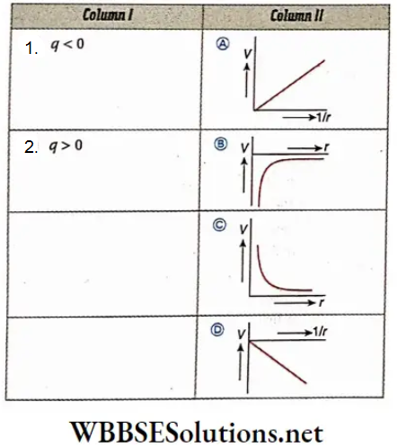
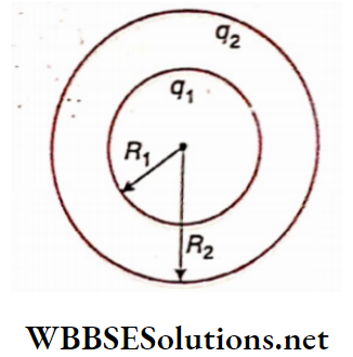
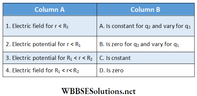
Question 1. Frequencies of a data signal lie between ω and ω’ (where (ω’ > ω) and the amplitude of the corresponding data signal is, v0 The data signal is superimposed on a carrier wave.

Communication System Signal Is Superimposed On Carrier Wave

Answer: 1-D, 2-C, 3- A, 4 – B

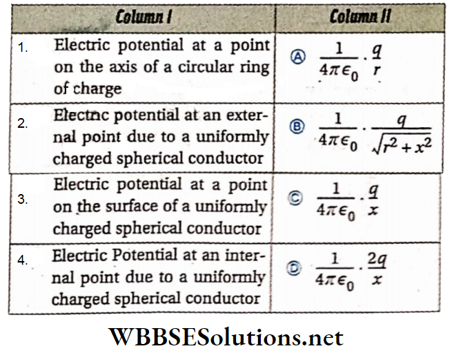
Question 2. For the communication system, the two columns (shown below) are to be matched

Communication System For Communication System

Answer: 1-C, 2-B, 3- A, 4 – D

WBCHSE Class 12 Physics Digital Electronics And Logic Gates Notes

WBCHSE Class 12 Physics Notes

Digital Electronics Introduction Analogue Signal And Digital Signal

The voltage or current signals passed through some traditional electronic circuits like a rectifier made of p- n junction diode or an amplifier made of the transistor can be varied continuously j within a definite range. For example. In the CE mode of a j transistor circuit, the input voltage can be varied continuously from j 0 V’ up to 6 Vor 10 V. This kind of signal is called an analog signal and (the corresponding electronic circuit is called analog circuit

On the other hand, In the case of ultra-modern electronic equipment like calculators, computers, etc., there are two discrete states of the Input or output signal low and high In this caw. the correct value of the voltage or current signal is not important at all. For example, If the magnitude of an input or output voltage lies in the range of 0 V to 0.5 V, it can be considered as j low voltage and if it lies between  V and 5 V, it can be j considered as high voltage. In this case, the circuit is so designed that the value of the voltage never lies in the range of 0.5 V to 4 V

WBCHSE Class 12 Physics Digital Electronics And Logic Gates Long Answer Questions

Read and Learn More Class 12 Physics Notes

If an electrical circuit exhibits input and output signals that can be categorised into two separate states, these states can be denoted by two symbols, usually in the form of two digits. This signal is classified as a digital signal, and the resulting circuit is called a digital circuit. A digital circuit is commonly known by this name. The utilisation of the circuit is less complex in contrast to that of an analogue circuit. The accuracy of the input and output signals is rather negligible. The latency between the input application and output acquisition is negligible, and the efficiency of this circuit is remarkably good. Given these factors, digital circuits are widely employed in the current period. In the realm of digital signals, the two discrete states are symbolised by two binary digits: 0 and 1. The numeral 0 represents a value that is considered to be low, whereas the numeral 1 represents a number that is considered to be high. Positive logic is the term used to describe the utilisation of digits.

In the above example, 0 is used as the symbol of voltage the voltage from 4 V to 0 5 V. On the other hand, in the case of less-used negative logic, l Is used to denote a low value and 0 Is used to denote a high value In different types of analog and digital signals, typical analog and digital signals respectively.

Here for analog signal, formation of wave i.e.. the actual form of time-varying voltage is most Important. On the other hand. In the case of digital signals, waveforms are always rectangular, i.e.. The interval of time In which the voltage is in a lower or higher state is Important. Thus the accuracy of the digital signal does not depend on the range or two discrete values of voltage In higher <uul lower state.

Digital Circuit Higher And Lower Gates

WBCHSE class 12 physics notes

Digital Electronics Number System

Binary system Definition: The system of expressing all the real numbers by the two digits 0 and 1 is called the binary system-

By a number, we usually mean a number in the decimal system. 10 digits—0, 1, 2, 3, 4, 5, 6, 7, 8, and 9 are used in the decimal system. Although in daily life decimal system is widely used. Computer circuits are fabricated by using a new system called binary number system which consists of two digits 0 and 1.

Let us consider a four-digit integral number 1101 in the binary system.

In this case, the places of the digits are given in the following table:

The value of any number depends on two factors:

  1. The magnitude and position of tire digits by which any number is formed and
  2. The base or radix ofthe number system. The base or radix of a number system refers to the number of digits used in the system.

For example, the bases of the decimal and binary systems are 10 and 2 respectively.

A number formed in a system is expressed by the symbol (number)base. For example, the number (257) formed in the decimal system is written as (257)10.  Similarly, the number (1101)2 formed in the binary system is written as (1101)2. The two numbers (11)10 and (11)2 are not the same; the first number is eleven and the second one is three.

WBCHSE class 12 physics notes Integers in Decimal and Binary Systems 

Decimal system:

Let us consider a four-digit integer 2795 in the decimal system. The number is expressed in words as two thousand seven hundred ninety-five. In this case, the places of the digits are given in the following table

Digital Circuit Decimal System Of Places

We can determine the value of this number from these places and from the base of the number system in the following way.

Or,

Digital Circuit From Base Of The Number System

= 2795

Digital Circuit Decimal System Of Number Places

The place of a digit indicates the significance of the digit. The digit lying at the extreme left- side of a number has the greatest significance and the digit at the extreme right has the least significance. In this case, the digit 2 has the greatest significance and hence 2 is the most significant digit. The digit 5 has the least significance and hence 5 is the least significant digit

Binary system:

Let us consider a four-digit integral number 1101 in the binary system. In this case, the places of the digits are given in the following table:

Digital Circuit Binary System Of Places Of The Digits

We can determine the value of this number in the following way:

Or,

Digital Circuit Determine The Value Of Number

= 13 ( decimal value)

WBBSE Class 12 Digital Electronics Notes

For a better understanding see the following table:

Digital Circuit Binary System Better Understanding Place Values

In the given number, the digit 1 in the place of 8 is the most significant digit and the digit 1 in the place of 1 is the least significant digit

Fractions In Decimal And Binary Systems

Decimal system:

A fraction in a decimal system is written by a decimal sign (.) and placed some digits right side of this sign. Such as .417. In this case, the places of the digits are given in the following table

Digital Circuit Binary System Places Of The Digits

The method of determining the value of the number is illustrated below with 0. 417 as an example

Or,

Digital Circuit Determining The Value Of The Number

= 0.417(decimal value)

For a better understanding see the following table:

Digital Circuit Decimal System Better Understanding

In the case of a fraction, the digit next to the decimal point is the most significant digit and the digit at the extreme right is the least significant digit. In this case, the digit 4 lying in the one-tenths place is the most significant digit and the digit 7 lying in the one-thousandth place is the least significant digit.

Logic Gates Class 12 Notes

Binary system:

Let us consider a fraction of 0.1011 in the binary system.

In this case, the positions of the digits are:

Digital Circuit Binary System Consider Fraction

The value of the number can be determined with the help of these places

The base of the number system is shown below:

Or,

Digital Circuit Binary System Place And BAse Of The Number System

= 0.6875 (Decimal value)

For a better understanding see the following table:

Digital Circuit Binary System Better Understanding See The Places

In the given fraction, the digit 1 in the place of \(\frac{1}{2}\) is the most significant digit and the digit 1 in the place \(\frac{1}{16}\) of is the least significant digit

Class 11 Physics Class 12 Maths Class 11 Chemistry
NEET Foundation Class 12 Physics NEET Physics

Binary to Decimal Conversion

The determination of the decimal value of any binary number was discussed in the previous section. Some examples of the conversion of binary to decimal numbers are given below:

1. (10111)2

= (1 × 24) + (0×23) + (1 ×22) + (1 ×21) + (1×20)

2. (10.111)2

= (1  × 21) + (0 ×20) + (1× 2-1) + (l ×2-12) + (1 × 2-3)

= 2 + 0 + 0.5 + 0.25 + 0.125 = (2.875)10

3.  (0.001)2 = (0 × 20) + (0 ×2-1) + (0 ×  2-2) + (1 × 2-3)

= 0 + 0 + 0 + 0.125 = (0.125)10

3.  (1.001 )2 = (1 × 20) + (0 × 2-1) + (0× 2-2) + (1× 2-3)

= 1 +0 + 0 + 0.125 = (1.125)10

Decimal to Binary Conversion

For better understanding, in the case of conversion of decimal to binary, it is necessary to discuss integers and fractions separately.

Conversion of integers:

Starting from 2°, the ascending powers of 2 are 20, 21, 22, 23, ………… Multiplying 0 or 1

With these numbers (i..e., 20,21 ……..) and then adding the \ products, any Integer can be expressed.

For example:

44 = (25 × 1) + (24 × 0) + (23 × 1) + (22 × 1) + (21 × 0) + (20 × 0)

45 = (25 × 1) + (24 × 0) + (23 × 1) + (22 × 1) + (21 × 0) + (20 × 1)

46 = (25 × 1) + (24 × 0) + (23 × 1) + (22 × 1) + (21 × 1) + (20 × 0)

47 = (25 × 1) + (24 × 0) + (23 × 1) + (22 × 1) + (21 × 1) + (20 × 1)

If we place those 0s and Is in order of their multiplication with the power of 2 to express the decimal number, the binary form of that decimal number can be easily expressed

So,

(44)10 = (101100)2

(45)10 = (101100)2

(46)10 = (101100)2

(47)10 = (101100)2

The process in which decimal numbers are converted into their respective binary numbers as discussed above, is not a correct mathematical process, because these calculations are done orally.

The proper method for conversion is to go on dividing the number and the successive quotients by 2 continuously, writing the remainder in each division till the quotient is zero. Arranging the remainders from bottom to top, i.e., from left side to right side, we get the given number in a binary system. Two examples are given below

1. Determination of the binary form of (44)10:

Digital Circuit Determination Of The Binay Form Of 44

2. Determination of the binary form of (45)10 :

Digital Circuit Determination Of 45

(45)10 = (101101)1

Logic gates class 12 notes Conversion of fraction:

Starting from 2-1, the descending powers of 2 are 2-1, 2-2, 2-3, ……… All fractions can not be expressed by multiplying 0 or 1 with these numbers (i.e. 2-1 2-2, ……. ) and then adding the products. For example, 0.125 = (2-1 × 0) + (2-2 × 0) + (2-3 × 1), but 0.12 cannot be expressed in this way.

Initially, it is necessary to multiply any decimal fraction by 2. If the product of the fraction is less than 1, write 0. If it is larger than 1, write 1. Place a binary point to the left of either 0 or 1. If the value of the fraction is less than 1, it must be multiplied by 2. If the value of the fraction is more than 1, just the non-integer part should be multiplied by 2. Similarly, if the value of this product is less than 1, assign it a value of 0; otherwise, assign it a value of 1.

The digit 0 or 1 must be placed immediately to the right of the preceding digit 0 or 1. Consequently, the decimal portion of the product value must be repeatedly multiplied by 2. Based on this criterion, input either 0 or 1 repeatedly until the product value reaches 1. However, in the majority of circumstances, the product value is not equivalent to 1. Therefore, it is not possible to represent the decimal fraction as an equivalent binary fraction. The process of converting a fraction from decimal to binary can be best comprehended through the following examples:

1. Determination of the binary form of 0.5625:

Digital Circuit Determination Of The Binay Form Of 0.5625

2. Determination of the binary form of 0.3:

Digital Circuit Determination Of The Binay Form Of 0.3

Short Notes on Digital Circuits

In this case, we see that the product can never be equal to 1 and part 1001 repeats again and again. So, 0.3 cannot be expressed in a binary fraction of the exact value. Since the part 1001 repeats itself in the fraction 0.010011001 …, it can be written as (0.0)(1001)2

∴ (0.3)10 = (0.0)(1001)2

It should be mentioned here that in case of any calculation, only those significant digits after the point are considered, which are required for the calculation. For example, if you require eight significant digits after the point for a calcula¬ tion, you should write,

(0.3)10 = (0.01001100)2

The integral and the fractional parts of any decimal number are converted separately into their corresponding binary values to express the number.

For examples:

(44)10 = (101100)2 and (0.5625)10 = (0.1001)2

∴ (44.5625)10 = (101100.1001)2

Addition, Subtraction, Multiplication, and Division of Binary Numbers:

The process of addition, subtraction, 1 multiplication, and division are similar for both decimal and binary systems. The only difference between binary and decimal.

The number is, in the decimal system, the numbers of digits are 10 (0, 1, 2, 9) whereas in a binary system, the number of digits 2(0 and 1).

Binary Addition:

Rule of Addition

0 + 0 = 0, 0 + 1 = 1 + 0 = 1,1 + 1 = 10

The last equation, 1 + 1 = 10 shows that, in a column, the sum of two binary’ 1 gives 0 in that column with a carry of1 in left

Example 1:

Digital Circuit Binay Addition Example 1

  1. In the first column (from right), the binary sum of 1 and 1 gives 0 in that column with a carry of in the left column (second column from right).
  2. In the second column (from right), the carry of1 from the first column is added to the sum of 1 and 0, giving 0 in that column with a carry of1 in the third column (from right).
  3. In the third column, the carry of 1 from the second column is added to the stun of 1 and 1, giving 11 in that column as there is no column in left

Example 2:

Digital Circuit Binary Addition Example 2

  1. In the first column (from right), the binary sum of 1, 1, 0, 1, and 0 gives 1 in that column with a carry of 1 in the left column (second column from right).
  2. In the second column, the carry of 1 from the first column is added to the sum of 0, 1, 1, and 1, giving 0 in that column with a carry of 10 in the third column from the right.
  3. HD In the third column, the carry of 10 from the second column is added to the sum of 1 and 1, giving 100 in that column as there is no column in the left.

Binary Subtraction:

Rule of subtraction

0 – 0 = 0, 1 – 0 = 1, 1 – 1 = 0, 10 -1 =

The tat three are the same as in decimal. The fourth rule is the only new one. It applies In the borrowing case when the top digit in

A column Is 0 and the bottom digit Is 1. (Remember: In binary, 10 Is pronounced as ‘one-zero’ or ‘two).

The procedure of binary subtraction is shown with an example in the table below : (Alter alignment of the numbers, subtraction proceeds from right to left)

Digital Circuit Binary Subtractions And Rules

Red marks indicate borrowing:

To subtract a large number from a small number,’ we subtract the small number from the large number and put a minus (-). sign before the result. Thus to subtract 11111 from 111001, we ‘ subtract the second number from the first number

Digital Circuit Substract Large Number From Small Number

As  11001 < 11111

So, 11001 – 11111 = -110

Important Definitions in Digital Electronics

Binary multiplication and division:

Rule of multiplication

0 × 0 = 0, 1 × 0 = 0 × 1= 0, 1×1 = 1

The process of binary multiplication is the same as decimal multiplication.

It should be mentioned here that in calculators and computers, multiplication and division are the same as repeated binary addition and subtraction. Hence in application, binary multiplication and division have no importance

Digital Electronics Number System Numerical Examples

Example 1. Write the decimal equivalent of (101101)2

(101101)2 = .1 × 25 + 0 × 24 + 1 × 23 + 1 × 22 + 0 × 21 + 1 × 20

= 32 + 0 + 0 + 4 + 0+1 =  (45)10

Example 2 Addition:

  1. (11001.101)2  + (1001.11)2 + (11.01)2
  2. (10000001)2 + (1111)2

Solution:

Digital Circuit Examples Of Additions

Example 3. Subtraction:

  1. (11001.101)2  –  (1001.11)
  2. (10000001)– (1111)2

Solution:

Digital Circuit Examples Of Subtraction

Logic gates class 12 notes 

Logic Gates

A gate is a special kind of digital circuit which possesses one or more input voltages but only one output voltage. OR, AND and

NOT gates are three basic gates. By joining these gates in different ways we can construct different kinds of circuits. These circuits perform arithmetic calculations and can conclude logical inferences like that performed by a human brain. This kind of mathematics was discovered by George Boole of England in 1854 AD. This form of mathematics is known as Boolean algebra.

Actual mathematical analysis of gates can be done with the help of Boolean algebra. Different gates can perform different algebraic processes and in this way, they can arrive at logical inferences. Thus, these gates are called logic gates or logic circuits

Boolean algebra:

To appreciate the importance of binary logic, let us consider, for example,

  1. Answer to a mathematical problem: is it ‘right’ or ‘wrong’?
  2. A physical statement: is it ‘true’ or ‘false’?
  3. Full a switch in a circuit: is it ‘on’ or ‘off’?
  4. The voltage across a circuit element: is it ‘low’ or ‘high’?
  5. A particle in a 2-level system: is it ‘up’ or ‘down’?

There are many situations in the physical world where only two such states are available. The method of explaining the truth by finding the answers of some two-valued questions related to a subject was first invented by the Greek philosopher Aristotle. Then some mathematicians understood that it is possible to express the method of finding the truth by the logic step by step by an algebraic method.

Notably, the British mathematician Augustus De Morgan discovered the interconnectedness between logic and mathematics. Subsequently, Bool carried out the remaining tasks. Nearly a century later, in 1938, the American applied mathematician employed this algebra for the first time in the telephone switching circuit.

Typically, the most practical method for representing these two states is by use a pair of numerical symbols, commonly 0 and 1. The decision of whether to employ 0 or 1 is referred to as binary logic. Boolean algebra is used to mathematically analyse a sequence of binary logical systems. The states of the input or output of a digital gate circuit are represented by the binary values of 0 or 1. Furthermore, a gate circuit can serve as a component of a sequence.

The output of a gate can serve as an input for the subsequent gate. Essentially, a digital gate circuit is a system that operates based on binary logic. Boolean algebra is the most suitable mathematical tool for analysing any circuit, regardless of its complexity, that is composed of digital gates.

An OR gate receives two or more input voltages or signals and produces a single output voltage or signal, similar to other types of gates. The gate is named OR gate because when any of the input voltages, whether it is the first, second, third, or any subsequent one, is high, the output voltage will also be high. For instance, if at least one of the input voltages of a two-input OR gate is in a high state, the output voltage of the gate will likewise be in a high state.

Working principle of OR gate: From the electrical analogy shown in Fig. 2.2, it becomes clear how an OR gate works. In this circuit, two switches A and B are connected in parallel. Obviously,

Digital Circuit Working Principle Of OR Gate

  • When both switches remain ‘off the bulb does not glow, i.e., the output becomes zero—no output is obtained.
  • One of the two switches, A or B, is ‘on’ but the other is ‘off; the bulb glows, i.e., a non-zero output is obtained.
  • If both switches are ‘on; the bulb glows and hence an output j is obtained.

So, this circuit works like an OR gate

OR gate in the electronic circuit:

An actual electronic two-input OR gate is the simplified form of this circuit. Two input voltages are denoted by A and, B and the output voltage is denoted by Y. Let the two possible states of the two input voltages below (say, 0 V) and high (say, 5V). The resistance RL is permanently connected to the circuit.

Digital Circuit OR Gate In Electronic Circuit

The gate may exist in any of the following four states:

  • Both A and B are low: In this case, the output voltage remains low. According to Fig. 2.3, if both A and B are low, the two diodes remain non-conducting. As a result, Y also remains low.
  • When A is low and B is high: In this case, the output voltage remains high.  If A is low, the diode attached to A remains in the non-conducting state. But if B is high, the diode attached to B is forward-biased, and hence Y remains high.
  • When A is high and B is low: In this case, the output voltage remains high. According to if B is low, the diode connected with B remains non-conducting. But if A is high, the diode connected with A is forward-biased, and hence Y remains high.
  • Both A and B are high: In this case, the output voltage remains high. According to if both A and B are high, the diodes connected with them are forward biased, and hence Y remains high.

OR gate Truth table:

A table can be prepared by taking the possible inputs and outputs of a gate. This table is called the truth table of that gate.

The truth table of a two-input OR gate is given here:

Digital Circuit Truth Table Of A Two Input OR Gate

As one of the inputs or the output of a gate can remain only in the two states low or high, this state can be easily expressed by binary digits. Expressing the lower state by 0 and the higher state by 1, the above truth table is prepared. By observing the truth table minutely, we understand that, if the state of any one of the two inputs is 1, the output state becomes 1. So, the state of Y becomes 1, if the state of either A or B or both A and B is 1.

In another way, we can regard an OR gate as an ‘any-or-all’ gate, i.e., the output state will be 1 if the states of any one or all inputs are I.

OR gate Positive and negative logic:

In the case of digital signal, if lower and higher states are represented by 0 and 1 respectively, it is called positive logic. On the other hand, If lower and higher states are represented by 1 and 0 respectively, it is called negative logic. Naturally, both positive and negative logic cannot be used simultaneously.

OR gate  Symbol: The symbol of an OR gate is Digital circuits can be drawn using this symbol

Digital Circuit OR Gate Symbol

Digital electronics class 12 notes 

Boolean algebra related to OR gate:

In Boolean algebra, the ‘OR’ operation is denoted by the symbol ‘+’ The Boolean algebraic equation related to the OR gate, shown in Fig. 2.5 is,

Y = A+B

This equation is read as: ” Y equals A OR B”.

When A = 0 = B, then Y = 0 + 0 = 0 .

When A = 0 and B = 1 , then Y = 0 + 1 = 1 .

When A = 1 and B = 0 , then Y = 1 + 0 = 1 .

When A = 1 = B, then Y = 1 + 1 = 1.

The equation 1 + 1 = 1 may appear to be absurd. But in Boolean algebra, the ‘+’ sign does not indicate addition. So, the equation 1 + 1 = 1 is read as “1 or 1 equals 1” For an OR gate circuit containing three inputs, the truth table, symbol, and Boolean algebraic equation are given below.

Digital Circuit Boolen Algebric Related Equation

Digital Circuit Boolean Algebra Related To OR Gate

AND Gate

In an AND gate, there are two or more input voltages or signals, and like any other gate, there is one output voltage or signal.

This gate is called AND gate because, If all the input voltages, i.e., the first the second, and the third und input voltages are high, only then will the output voltage be high. For example, if Both the input voltages of a two-input AND gate are high, then only its output voltage will be high.

Digital electronics class 12 notes Working principle of AND gate:

From the electrical analog) it becomes clear how an AND gate works.

Digital Circuit Working Principal Of AND Gates

  1. In this circuit, two switches A and B are connected in series. Obviously,
  2. When both the switches remain ‘off; the bulb does not glow, i.e., output becomes zero — no output is obtained.
  3. One of the two switches, A or B, is ‘on’ but the other is ‘off,’ even then the bulb does not glow, i.e., output becomes zero no output is obtained.
  4. Sial only when both the switches arc ‘on,’ the bulb glows, i.e., the output is obtained.

So, this circuit works like an AND gate

AND gate In the electronic circuit:

An actual electronic j two input AND gate Is The simplified form of j earthing. This circuit. The two input voltages are denoted by A and B, and the output voltage by Y. Let the two possible states of the two Input voltages below (say, 0 V) and high (say, 5 V). The resistance Rj and the battery VCC (= 5 V); are permanently connected with the circuit.

Digital Circuit AND Gate In The Electronic Circuit

Digital electronics class 12 notes 

The gate may exist in any of the following four states:

  1. Both A and II arc low: In this case, the output voltage remains low. According to if both A and R are low, due lo VCC the two diodes are forward biased, i.e., two diodes are Conducting. As a result, the voltages of A, B, and Y are the same, I.e., Y Is also low.
  2. If A low and B it high: In this case, the output voltage is low. According to if R Is high, the diode connected with R is reverse biased, l.e„ this diode Is Non-conducting. Rut If A Is low, due to the diode connected with A Is forward biased, I.e., this diode is Conducting. As a result, the voltages of A and Y are the same, i.e., Y is low.
  3. If A is high and B is low:
  4. In this case, the output Is low The reason for this Is similar to that described In 2 above.
  5. Both A and B are high: In this case, the output Is high. According to if both A and B are high, the two diodes are reverse biased, I.e., the diodes arc in the non-conducting state. As a result, no current flows through RL, and hence due to VCC, the output Y Is high.

By comparing, we can see that an Or gate easily becomes an AND gate if we alter the ends of the diodes and achieve a proper voltage (Vcc) at one end of RL instead of earthing

AND gate Truth table:

Observing the truth table carefully, we understand that. If the states of both the Inputs be l. the state of the output will be I. So, the state of V’ will be 1 If states of both A and R arc I. lit another way, we can regard an AND gate as an all or none gate i.e the out state will be 1 if the states of all input be 1 otherwise output state will be 0.

Digital Circuit AND Truth Table

AND gate Symbol: The symbol of an AND gate Is shown in the Digital circuits that can be drawn using this symbol.

Digital Circuit This Equivalent To An AND Gate Y

Boolean algebra rotated to AND gate:

In Boolean algebra, ‘AND’ operation Is denoted by the symbol the Boolean algebraic equation related to AND gate, shown in

Y= A.B = AB

This equation is read as: ” Y equals A AND B”.

When A = 0 = B, then 7= 0.0 = 0

When A = 0 and B = 1 , then 7= 0 .1 = 0

When A = 1 and 5 = 0, then 7=1.0 = 0

When A = 1 = 5, then 7=11 = 1.

A three-input AND gate circuit, its truth table, symbol and

Boolean algebraic equations are given below:

Digital Circuit Boolean Algebra Related AND Gate

Digital Circuit Boolean Algebra Related To AND Gate

Logic gates physics class 12 

AND gate Digital Signal: The waveforms of two digital signals A and B are

  • For OR gate – A + B= Y: In time intervals EF and GH, both signals A and 5 are in a lower state i.e., 0. So, for these time intervals, output 7 of the OR gate will be 0. For all other intervals, A or 5 or both A and 5 are in a higher state, i.e., 1. Hence, output state 7 will be 1. This output waveform

Digital Circuit Digital Signal For OR Gate

  • For AND gate – AB = Y: In this case, signals A and B are in a higher state i.e., 1 for the time intervals CD, FG, and IJ So, for these time intervals, the output of the AND gate will be in a higher state i.e., 1. For all other intervals, A or 5 or both A and 5 are in a lower state i.e., 0. Thus output 7 will be in a lower state ) i.e., 0. This output waveform.

NOT Gate

In a NOT gate, there is one input and one output voltage or signal. This gate is called NOT gate because the states of the output voltage and input voltage can never be the same. So, if the input voltage in a NOT gate is low, the output voltage will be high and vice versa. This gate is also known as an inverter.

Working principle Of NOT gate:

From the electrical analogy it becomes clear how a NOT gate works. In this circuit, a switch A and a bulb are connected in parallel.

Clearly,

  1. When the switch remains off, the bulb glows, i.e., an output is obtained.
  2. When the switch remains on, the bulb does not glow, i.e., output becomes zero — no output is obtained. So, this circuit works like a NOT gate

Digital Circuit Working Principle Of NOT Gate

NOT gate in the electronic circuit:

An actual electronic NOT gate. The simplified form of this gate. Note that, diodes cannot form a NOT gate; at least one transistor is necessary.

Digital Circuit NOT Gate In Electronic Circuit

Here, the input and the output voltages are denoted by A and 7 respectively. Let the two possible states of the input and output

Voltages are low (say, 0 V) and high (say, 5 V). Two resistances RB and RC and the battery Vcc (= 5V) are connected permanently to the circuit.

Digital Circuit NOT Gate In Electronic Circuit Exist States

Logic gates physics class 12 

The gate can exist in any of the two states given below:

  1. A is low: In this case, the output voltage is high. According to, Fig. 2.14, if A is low, the values of Rg and Rc are so chosen that the transistor is in the cut-off region, i.e., almost no current passes through the transistor. As a result, Y remains high due to Vcc.
  2. A high: In this case, the output voltage is low. According to Fig. 2.14, if A is high, due to Rg and Rc, the transistor is in the saturation region, i.e., maximum current flows through Rc. As a result, the point P is in a low state, i.e., Y is low

NOT gate Truth table:

Digital Circuit Truth Table Of The NOT Gate

NOT gate Symbol:

The symbol of a NOT gate. Digital circuits can be drawn by using this symbol.

Digital Circuit NOT Gate Symbol

Boolean algebra related to NOT gate:

In Boolean algebra, the ‘NOT’ operation Is denoted by giving a ’ sign above A. The Boolean algebraic equation related to NOT gate, shown

Y = \(\bar{A}\)

This equation is read as: “ Y equals NOT A ”

When A = 0 , then Y = \(\bar{0}\) = 1.

When A = 1 , then Y = \(\bar{1}\)  = 0.

NOT output of a digital Input:

According to each lower state I.e., 0 of the input signal A (in time intervals DF and GH), the output Y remains in the higher state the other hand, for higher state of A i.e., 1 (in time Intervals CD, FG, and HJ), the output Y remains in lower state i.e., 0

Digital Circuit NOT Output Of A Digital Input

  • OR, AND, and NOT gates are called basic logic gates because, any other logic gate is the combination of these three basic gates, In any manner.
  • A logic gate cannot be formed by using any one of the basic gates repeatedly. For example, combining a large number of OR gates, no AND gate or NOT gate can be constructed.
  •  The NOR gate and the NAND gate, discussed in the next section have some special advantages. A logic gate of any kind can be constmcted by a combination of any number of NOR gates or NAND gates only. Thus, NOR and NAND gates are called universal logic gates, although none of them are basic gates.
  • To construct different logic gates by using more than one basic gate, DC Morgan’s theorem can hr applied.
  • Dc Morgan’s theorem:
    1. \(\overline{A+B}=\bar{A} \cdot \bar{B}\)
    2. \(\overline{A \cdot B}=\bar{A}+\bar{B}\)

Logic gates physics class 12 NOR Gate

Joining the Input of a NOT gate with the output of an OR gate, a NOT-OR, i.e., a NOR gate is constructed So, the voltage or signal that comes at the output of an OR gate, goes to die input of a NOT gate. NOT gate Inverts this voltage and sends it to the output.

NOR Gate Truth table:

In the case of a NOR gate, only if the states of all of the Inputs are 0, the output state becomes 1.

Digital Circuit NOR Gate Truth Table

Digital Circuit NOR Gate Truth Table Y

NOR gate Symbol:

Two symbols of a NOR gate are. Digital circuits can be drawn by using any one. The second symbol is more commonly used

Boolean algebra related to NOR gate:

The Boolean algebraic equation related to the NOR gate

This equation is read as Y equals A NOR B”

When.A = 0 r: B, then V = \(\overline{0+0}\) = 1.

When A = 0 and B = 1 , then , Y = \(\) = 0.

When A = 1 and B = 0 . then Y = \(\overline{1+0}\) = 0.

When A – 1  and B = 1 . then Y = \(\overline{1+1}\) = 0.

Design of basic gates using one or more NOR gates:

1. From NOR gate to OR gate:

Digital Circuit NOR Gate To OR Gate

2. From NOR gate to AND gate:

Digital Circuit NOR Gate To AND Gate

3. From NOR gate to NOT gate:

Digital Circuit Design Of Basic Gates Using NOR Gate To NOT Gate

NAND Gate

Joining the input of a NOT gate with the output of an AND gate, a NOT-AND, i.e., a NAND gate is constructed. So, the voltage or signal that comes at the output of an AND gate, goes to the input of a NOT gate. NOT gate inverts this voltage and sends it to the output.

NAND Gate truth table:

In case of a NAND gate, if the state of any of the inputs be 0, the output state becomes 1.

Digital Circuit NAND Truth Table

Digital Circuit NAND Gate Truth Table Y

NAND Gate Symbol:

Two symbols of a NANI) gate arc shown In Rig. 2.22. Digital circuits can ho drawn using any one. The second symbol Is more commonly used

Boolean algebra related to NAND gate:

The Boolean algebraic equation related to the NAND gate,

This equation is read as: ” Y equals A NAND It”.

When A = 0 = B,  then Y = \(\overline{0.0}\)  = 1 .

When A = 0 and B = 1 , then Y = \(\overline{0.1}\) = 1
.
When A = 1 and B = 0 , then Y = \(\overline{1.0}\) = 1.

When A = 1 and B = 1 , then Y = \(\overline{1.1}\) = 0

Design of basic gates using one or more NAND gates:

1. From NAND gate to OR gate:

Digital Circuit Design Of Basic Gates Using NAND Gate To OR Gate

2. From NAND gate to AND gate:

Digital Circuit Design Of Basic Gates Using NAND Gate To AND Gate

3. From NAND gate to NOT gate:

Digital Circuit NAND Gate To NOT Gate

Digital electronics and logic gates notes 

NOR and NAND outputs of two digital inputs:

The waveforms of two digital signals A and B are as an example.

Digital Circuit NOR And NAND Outputs Of Two Digital Inputs

  • For NOR gate \(\overline{A+B}\)  = Y: In time intervals EF and GH, both the signals A and B are in a lower state i.e., 0. So, for these two-time intervals, the output Y of the NOR gate will be in a higher state i.e., 1. For all other intervals, A or B or both A and B are in a higher state i.e., 1. Hence, the output state Y will be 0. This output waveform.
  • For NAND gate \(\overline{A \cdot B}\) = Y: Here, for the time intervals CD, FG, and IJ, both the signals A and B are in a higher state i.e., 1. So, for these intervals, output Y of the NAND gate will be in a lower state i.e.„ 0. On the other hand, for all other intervals, A or B or both A and B are in a lower state i.e., 0. Hence output state Y will be 1. This output waveform

Some Relations of Boolean Algebra

Verification of the following relations of logic signal A, by putting A = 0 and A = 1 in each of these relations

Digital Circuit Some Relations Of Boolean Algebra

Some other useful theorems:

A + AB = A

A + \(\bar{A}\) = A + B

A(A + B) = A

A + (\(\bar{A}\)) = A + B

A(A + B) – AB

Three Laws of Boolean Algebra

Commutative law: A + B = B+A; AB = BA

Associative law: A + (B+ C = (A+B) + C

A . (B. C) = (A . B). C

Distributive law: A.(B+C) = A. B + A.C

Digital electronics and logic gates notes 

Determination of Boolean Algebraic Relation and Design of Logic Circuit from Truth Table

To understand the process of determination of Boolean algebraic relation, first, we shall discuss a truth table as an example is given below:

Digital Circuit Determination Of Bolean Algebraic Relation And Design Of Logic Circuit From Truth Table

Here, we consider the rows in which Y = 1. So, the second and third rows of the table are taken into consideration. The first and fourth rows are ignored.

In second row, for A = 1, write A, and for B = 0, write B. The Combined relation of these two will be AB. Again in the third row, for A = 0, write \(\bar{A}\), and for B  = 1, write B.

The combined relation of these two will be \(\bar{A}\) B. As Y = 1 for A\(\bar{B}\) OR \(\bar{A}\)B, so, the Boolean algebraic relation will be Y = A\(\bar{B}\) + \(\bar{A}\)B.

The logic circuit associated with this Boolean relation is. Here, by using the NOT gate, input A is converted to \(\bar{A}\). In the same way, input B is converted to \(\bar{B}\).

Now, A and B are applied as inputs to an AND gate. Similarly, \(\bar{A}\) and B are applied as inputs to another AND gate The outputs of these two AND gates are A\(\bar{B}\) and \(\bar{A}\) B respectively. These outputs are applied to an OH gate as inputs. Then, the final output will be V =  \(A \vec{B}+\overline{A B}\)

Digital Circuit Exclusive OR Gate Or XOR Gate

In the Practice field, this gate is known as an Exclusive- OR or XOR. For example, two-way switching in which two switches are used to control a bulb or a fan in a house.

In this system, a bulb or a fan is connected in such a way that if any one of these two switches is in an ‘on’ state, the current will flow through the bulb or the fan. But if both of these two switches are in the ‘on’ or ‘off’ state, then no current will flow i.e., the die bulb or the fan will be in the ‘off state. This type of circuit system is an XOR gate.

Examples of Digital Circuit Applications

Example 1: Truth table of AND gate:

The given truth table shows that Y = 1 in only die fourth row of the table. Hence the rest of the rows need not be taken into consideration.

In the fourth row, for A = 1 , write A, and for B = 1, write B. As A = 1 AND 5=1, so, final Boolean algebraic relation is Y= AB

Digital Circuit Truth Table Of And Gate

From above, it is clear that this is well known Boolean algebraic relation of AND gate. Hence the corresponding logic circuit is an AND gate.

Digital Circuit AND Gate

Conceptual Overview of Boolean Algebra

Example 2: The truth table of OR gate:

The given truth table shows that Y = 0 in only the first row of the table. Hence excluding the first row, we see that for the second row, the relation is AB; for the third row, the relation is A\(\bar{B}\) and the relation for the fourth row is AB.

Digital Circuit Truth Table Of OR Gate

Digital Circuit Truth Table Of OR Gate

So, for Y = 1, the relation will be A \(\bar{B}\) OR  \(\bar{A}\) B OR AB. Hence the Boolean algebraic relation for the given truth table is Y =  \(A \bar{B}+\bar{A} B+A B\)  + AB. The corresponding logic circuit is shown below.

By simplifying the relation:

Y = \(A \bar{B}+\bar{A} B+A B\)

= \(A \bar{B}+(\bar{A}+A) B=A \bar{B}+B\)

= \(A \bar{B}+(A+1) B \quad\{ A+1=1 \mid\)

= \(A \bar{B}+A B+B=A(\bar{B}+B)+B\) =

= A+B \(A+B \quad \bar{B}+B=1]\)

This is the well-known Boolean relation of the OR gate. Hence the corresponding logic circuit is an OR gate. So, the circuit is equivalent to a two-input OR gate.

Digital Electronics And Logic Gates Integrated Circuit Or IC

Until recently, it was customary to construct electronic circuits with passive components such as resistors, capacitors, and inductors and active components such as diodes and transistors connected by conducting wires. In practice, however, such circuits have two major disadvantages.

1. Connection problem:

The connection between the various components has to be done necessarily by soldering the wire to the element. Naturally, there are chances of solving leading to the entire circuit being rendered useless. This defect is also very difficult to remove because itis practically impossible to locate the defective soldering joints.

Digital Circuit Connection Problem Of Soldering Joints

2. Size of the circuit:

Most often complex electronic circuits comprising of a large number of elements are necessary. This causes an unusual increase in the size and production cost of the electronic instrument.

In later years, an integrated circuit(IC), was invented by physicist JG Kilby played a remarkable role in removing these disadvantages in manufacturing electronic circuits, As IC is just a small bit of silicon crystal or chip.

The relative advantages and disadvantages of an IC , over discrete electronic circuits are brief or chip.

Tim relative advantage and disadvantages of an IC over (discrete l electronic circuits arc briefly stated below

IC Advantages:

  1. No soldering Is necessary, The entire connection Is built up inside the IC. Hence It Is very reliable,
  2. In possible to build up a large number of electronic components within a single chip, 10 used In INTEL PENTIUM microprocessor consists of more than ten lakh electronic components,
  3. Due to Its small size, the cost Is very low, Hence replacement Is better than repairing a defective element
  4. Due to small size and Jow costing, sufficiently complex circuits are possible to construct using IC which also increases the efficiency of the circuits.

IC Disadvantages:

  1. It is impossible to fabricate transformers or any other kind of inductor onto the integrated circuits. (~in Power rating of IC is sufficiently low; besides this, it cannot withstand high fluctuation of voltage or temperature.
  2. If hulk production is not done instead of small-scale production, it is not commercially viable. Moreover, advanced technology is essential for the production of perfect ICs.
  3. Still, it can be safely remarked that the advantages of IC far outweigh the disadvantages which are being brought under effective control with the help of superior technology.

IC Classification:

Based on their working principle and uses, ICs are classified into two types.

  1. Linear or analog IC: Here the relation between input and output is linear. Also, the input and output voltages and curpioTJoyi rents change continually within a certain range. Linear IC is used in amplifiers, oscillators, and especially in operational amplifiers (OPAMP).
  2. Digital IC: In this type, input and output voltages can have only two states either high or low. No continuous change occurs in this voltage or current. Digital IC is used in simple digital circuits, microprocessors, etc.

Digital Electronics And Logic Gates Synopsis

1. If the input and the output signals of an electronic circuit have two discrete states, they can be denoted by two digits. These kinds of signals are called digital signals and the circuits are called digital circuits.

2. The system of expressing all the real numbers by the two digits 0 and 1 only, is called a binary system.

3. With the help of Boolean algebra, mathematical analysis of gate circuits can be done and the different gates can perform different algebraic processes. In this way, they can arrive at logical Inferences. These gates are known as logic gales or logic circuits.

The fundamental logic gates are OR, AND, and NOT gates.

4. The Boolean algebraic equation of a 2-Input OR gate is,

Y = A+B

5. The Boolean algebraic equation of a 2-input AND gate is,

Y = A.B

6. The Boolean algebraic equation of a NOT gate is,

Y = \(\bar{A}\)

7. The Boolean algebraic equation of a 2-input NOR gate is

Y = \(\overline{A+B}\)

8. The Boolean algebraic equation of a 2-input NAND gate is

Y = \(\overline{A \cdot B}\)

9. NOR and NAND gates are called universal logic gates.

10. De Morgan’s theorem related to Boolean algebraic relations:

  1. Y = \(\overline{A+B}=\bar{A} \cdot \bar{B}\)
  2. Y = \(\overline{A B}=\bar{A}+\bar{B}\)

11. Each IC is a very small single block or chip of silicon crystal in which several electronic circuit components (e.g. transistors, diodes, resistors, etc.)

12. Are electrically interconnected and their interconnections form a complete electronic circuit Hence, an IC performs a complete electronic function

Digital electronics and logic gates notes 

Digital Electronics And Logic Gates Very Short Question And Answers

Question 1. Of the two binary numbers, 10010111 and 10011001, which one is the greater?
Answer: 100111001

Question 2. Of the two numbers (10)10 and (11)2, which one is the greater
Answer: (10)10

Question 3. What is radix in decimal and binary systems respectively?
Answer: 10, 2

Question 4. (33)10 = (____________)2 . =
Answer: 100001

Question 5. Is it possible to convert an analog circuit into a digital circuit
Answer: Yes

Question 6. Is it possible to convert a digital circuit into an analog circuit?
Answer: Yes

Question 7. If A and B are the two inputs of an AND gate, what will be the value of the output?
Answer: A.B

Question 8. What role will an AND gate play if negative logic is used instead of positive logic
Answer: OR gate

Question 9. When in Input signal 1 Is applied to a NOT gate. What will be its output?
Answer: 0

Question 10. If the output of a NOR gate Is fed to the Input of a NOT gate then this combination will be called what
Answer: 1

Digital Electronics and Logic Gates Assertive Type

  1. Statement 1 is true, statement 2 Is true; statement 2 Is a correct explanation for statement 1.
  2. Statement 1 is true, and statement 2 Is true; statement 2 is not a correct explanation for statement 1.
  3. Statement 1 Is true, and statement 2 Is false.
  4. Statement 1 Is false, and statement 2 Is true.

Question 1.

Statement 1: The conversion of binary number 1101 to decimal number can be written as 24+ 23 +  0+ 21 = 26

Statement 2: In a binary system, the base is 2, and the digits used are 0 and 1

Answer: 4. Statement 1 Is false, statement 2 Is true.

Question 2.

Statement 1: The conversion of binary fraction 0 101 to decimal fraction can IK* written as 2-1 + 0 + 2-3 = 0.625

Statement 2: In a binary system, the base is 2, and the digits used are 0 and 1.

Answer:  1. Statement 1 is true, statement 2 Is true; statement 2 Is a correct explanation for statement 1.

Question 3.

Statement 1: OH gate is a basic logic gate

Statement 2: Any logic gate can be made  by using more than one OK gate in an appropriate combination

Answer: 3. Statement 1 Is true, and statement 2 Is false.

Question 4.

Statement 1:  NOR gate is a basic logit: gate.

Statement 2: Any logic gale tan he made by using more than one NOR gate In appropriate combination.

Answer: 4. Statement 1 Is false, statement 2 Is true.

Question 5.

Statement 1: Boolean algebraic equation oI NOT gate Is
Y = \(\bar{A}\)

Statement 2: NOT gate is used to Invert the state of a digital signal between Its two states.

Answer:  1. Statement 1 is true, statement 2 Is true; statement 2 Is a correct explanation for statement 1.

Question 6.

Statement 1: According to Boolean algebra,2

Statement 2: The output of an AND gate becomes ‘on’ only if all the Inputs remain In the ‘on’ state.

Answer: 2. Statement 1 is true, and statement 2 Is true; statement 2 is not a correct explanation for statement 1.

Question 7.

Statement 1: The decimal value of  the binary number 111 is 7 therefore (0.11) = (7/2³)10

Statement 2: Decimal fraction 0.1 1 1 can be written as (111/10³)

Answer: 1. Statement 1 is true, statement 2 Is true; statement 2 Is a correct explanation for statement 1.

Digital electronics and logic gates notes 

Digital Electronics and Logic Gates Match The Columns

Question 1. Some decimal numbers and their corresponding binary values are given column 1 and column 2 respectively
Answer:

Digital Circuit Decimal Numbers And Its Corresponding Binary Values

Answer: 1-D, 2-B, 3-A, 4-C,

Question 2. Match the logic gates in column 1 with truth tables in column 2

Digital Circuit Logic Gates

Answer: 1-B, 2-C, 3-D, 4-A,

Question 3. Some logic gates and their corresponding Boolean algebraic equations are given in column 1 and column 2 respectively

Digital Circuit Some Logic Gates And Its Corresponding Boolean Algebraic Equations

Answer: 1-C, 2-A, 3-D, 4-B,

WBCHSE Class 12 Physics Digital Electronics & Logic Gates Long Answer Questions

Digital Electronics & Logic Gates Long Question And Answers

Question 1. What are the differences between analog circuits and digital circuits?
Answer:

Digital Circuit Difference Between Analogue Circuit And Digital Circuit

Read And Learn More WBCHSE Class 12 Physics Long Question And Answers

Question 2. Given a battery, two switches, and an electric bulb, how can

  1. An OR gate and
  2. An AND gate be constructed?

Answer:

If the switch is made on or off, the bulb glows or extinguishes. Hence, the two switches are the inputs, and the d bulb is the output

Digital Circuit Given A Battery Two Switches And An Electric Bulb

  1. The circuit is an OR gate circuit because when any one or both the switches, A and B are on, bulb Y will glow.
  2. The circuit is an AND gate circuit because only when both switches A and B are on, are the bulb Y glows.

WBCHSE Class 12 Physics Digital Electronics And Logic Gates Short Answer Questions

Question 3. Given a battery, a switch, and an electric lamp, how can a NOT gate be constructed?
Answer:

In this case, the switch is the input, and the electric bulb is the output, because when the switch is made ‘on’ or ‘off’ then the lamp goes ‘off’ or ‘on’ respectively. The circuit is a NOT gate circuit. When switch A is off, current flows through the lamp Y and it glows. When the switch is on, the entire current passes through the arm of the switch. As a result, the bulb extinguishes.(To avoid short circuits a low value resistance may be concentrated with switch A.

Digital Circuit Given Battery A Switch And An Electric Lamp

WBBSE Class 12 Digital Electronics Long Answer Questions

Question 4. Write down the truth table of the following circuit.

Digital Circuit Truth Table Of The Circuit

Answer:

Digital Circuit Truth Table Of Circuit

Digital Circuit Truth Table Of Circuit.

Practice Long Answer Questions on Combinational Circuits

Question 5. What is the value of Y shown in the circuit given below?

Digital Circuit Value Of Y Circuit

Answer:

The output of the OR gate at the left-hand top is 1 and the output of the AND gate at the bottom is 0. These values change to 0 and 1, respectively after they pass through the two NOT gates.

Lastly, when it passes through the OR gate at the extreme right, the final output becomes, Y = 0 + 1 = 1

Y = \(\overline{1+0}+\overline{1 \cdot 0}\)

= \(\overline{1}+\overline{0}=0+1\)

= 1

Question 6. In the given circuit diagram, If the output Y = I, what are the three inputs A, B, and C?

Digital Circuit Given Circuit Are The Three Inputs

Answer:

For Y = 1, the two inputs of the AND gate on the right-hand side must be 1. Of them, the input at the top will be 1 if both A and B are 1; the input at the bottom will be 1 if C = 0. So, A = 1,B = 1,C = 0.

Alternative Answer:

Digital Circuit Decimal Alternative Table

From truth table, it can be inferred that if A = 1 , B = 1 and C = 0 , then Y = 1

Question 7. An OR gate is operated by using positive logic. What role will the OR gate play if we use negative logic? Or, Show that the truth table of an OR gate in negative logic is similar to that of an AND gate in positive logic.
Answer:

In positive logic, lower and higher states are denoted by 0 and 1 respectively. According to this, the truth table of the OR gate is

  1. On the other hand, in negative logic, lower and higher states become 1 and 0 respectively. For this, 0 and 1 interchange their positions in the truth table. So, the new truth table
  2. Will be the same as the truth table of an AND gate in positive logic.

1. 

Digital Circuit OR Gate is Operated By Using Positive Logic

2. 

Digital Circuit AND Gate Positive Logic

Important Definitions in Digital Electronics

Question 8. How would you construct a NOT gate by using a NOR gate?
Answer:

Signal A has been divided into parts and applied simultaneously and the two Inputs of the NOR gate G. Out¬ put Y is shown In the truth table. It may be noticed that this table is the same as the truth table of NOT gate. So, it is possible to make a NOT gate by using a single NOR gate.

Digital Circuit NOT Gate By Using A Single NOR Gate

Digital Circuit Single NOR Gate

Class 11 Physics Class 12 Maths Class 11 Chemistry
NEET Foundation Class 12 Physics NEET Physics

Question 9. The waveforms of two digital signals A and B are.  If we apply these two signals A and B to an OR gate as inputs, then what will be the output waveform

Digital Circuit Wave From Two Digital Signals A And B

Answer:

Digital Circuit Decimal Time intervals

In different intervals of time, possible combinations of values 0 or 1 of A and B are shown in the truth table. From the truth table, the waveform of the output Y is

Digital Circuit Wave From Of The Out Put Y

Question 10. Waveforms of two inputs A and B and output Y are. Find the Boolean algebraic equation of the associated logic gate and draw the circuit diagram of it.

Digital Circuit Waveforms Of Two Inputs A And B And Out put

Answer:

From the given waveforms, we get the following truth table.

Digital Circuit Waves From Two Inputs A And B And Output Y

Digital Circuit The Circuit Diagram Of Logic

For this truth table, the Boolean algebraic equation of the associated gate is Y = A. The circuit diagram of associated logic

Question 11. Write the Boolean expression and the truth table for the logic circuit which is given

Digital Circuit Boolean Expression For The Logic Circuit

Answer:

In this, we see that a NAND gate is followed by another NAND gate. Signals A and B are applied to the first NAND gate as inputs. Then the output of the first NAND gate AB is fed simultaneously to both inputs of the second NAND gate.

The output of the second NAND gate is AB i.e., AB. So, this logic circuit will act as an AND gate.

Hence, the Boolean algebraic equation is Y = AB.

The truth table of the given logic circuit is as follows:

Digital Circuit Boolean And The Truth Table The Logic Circuit

Question 12. Write the Boolean expression and truth table for the logic circuit which is 

Digital Circuit Boolean Expression And Truth Table

Answer:

The Boolean expression for the given logic circuit is

Y= AB +\(\overline{A B}\)

The truth table of the given logic circuit is as follows:

Digital Circuit Boolean Expression For Logic Circuit

Examples of Logic Circuit Design Questions

Question 13. Find the Boolean expression of the given logic circuit. Draw the simplest logic circuit equivalent to this given logic circuit.

Digital Circuit Simplest Logic Circuit Equivalent

Answer:

The Boolean expression for the given logic circuit is

Y= A+\(\bar{A B}\)

Now, Y = A + \(\overline{A}\) B = A . 1+\(\overline{A}\) B = A(1+ B) +\(\overline{A}\) B

= A+ AB + \(\overline{A}\) B

= A + (A +\(\overline{A}\)  )B = A + 1 .B

∴ Y = A + B

Hence, the equivalent circuit is an OR gate

Question 14. Two digital signals A and B shown in Fig. 2.46 are used as the two Inputs of 

  1. OR 
  2. AND
  3. NOR and
  4. NAND gate.

Obtain the output waveforms in each of the four cases

Digital Circuit Two Digital Signals A And B Output Waveforms

Answer: From the given waveforms, we get the following truth table

Digital Circuit Time Interval Of Input And Output

From this truth table, the output waveforms in each of the four cases are

Digital Circuit The Output Waveforms In Each Of The Four Cases

Question 15. The required AND gate ( Y = AB).  Find the Boolean expression of the given logic circuit. Draw the simplest logic circuit equivalent to this given circuit.

Digital Circuit Draw The Simplest Logic Ciecuit Eqivalent Given The Circuit

Answer: The Boolean expression for the given logic circuit is

Y = \(\bar{A}+\overline{A B}\)

Now, Y = \(\bar{A}+\overline{A B}\)

= \(\bar{A}+\bar{A}+\bar{B}\)

[∴  From De Morgan’s theorem, AB = A + B]

= \((\bar{A}+\bar{A})+\bar{B}=\bar{A}+\bar{B}\)

Y =\(\bar{A}+\bar{B}=\overline{A B}\)

Hence, the equivalent circuit is a NAND gate

Question 16. Find the Boolean expression from the given truth table and draw its simplest logic circuit

Digital Circuit Boolean Expression Simpest Logic Circuit

Answer:

Here, Y = 1 in only the first row of the truth table. Thus rest of the rows are not taken into consideration. In the first row, for A = 0 AND B = 0, write AB. Therefore, the Boolean expression is Y = \(\).

According to De Morgan’s theorem,

⇒ \(\overline{A+B}=\bar{A} \bar{B}\).

So, Y = \(\overline{A+B}\). It is the Boolean expression of the NOR gate. Hence, ‘ the simplest logic circuit is a NOR gate

Digital Circuit Simplest Logic Circuit Is A NOR Gate

Question 17. How would you construct an AND gate by using mini¬ mum number of OR and NOT gates?
Answer:

Here, we have to use the following relations.

⇒ \(\bar{A}+\bar{B}=\overline{A B} \text { and } \overline{\overline{A B}}\)

The required AND gate ( Y = AB) is

Digital Circuit The Required The AND Gate

Question 18. Find the Boolean expression from the given truth table and draw its simplest logic circuit.

Digital Circuit Boolean Expression Of The Truth Table
Answer:

Here, Y = 1 in the first, second, and third rows of the truth table. Thus these three rows are to be taken into consideration.

For the first row, the Boolean expression is \(\bar{A} \bar{B}\). (∴  A = 0, B = 0 ),

For the second row, the Boolean expression is  \(A \bar{B}\) (∴A = 1, B = 0) and

For the third row, the Boolean expression is \(\bar{A} B\) ( ∴ A = 0, B = 1 ).

So, the complete Boolean expression is Y = \(\bar{A} \bar{B}+A \bar{B}+\bar{A} B\)

By simplifying, we get,

Y = \(\bar{A} \bar{B}+A \bar{B}+\bar{A} B=(\bar{A}+A) \bar{B}+\bar{A} B\)

= \(1 \cdot \bar{B}+\bar{A} B\)

Since  \(\bar{A}\) + A = 1

= \(\bar{B}+\bar{A} B=(1+\bar{A}) \bar{B}+\bar{A} B\)

Since 1  + \(\bar{A}\) = 1

= \(\bar{B}+\bar{A} \bar{B}+\bar{A} B\)

= \(\bar{B}+(\bar{B}+B) \bar{A}=\bar{B}+\bar{A}\)

i.e Y  = \(\bar{A}+\bar{B}=\overline{A B}\) According to De Morgans theorem

It is the Boolean expression of the NAND gate. Hence, the simplest logic circuit is a NAND gate

Question 19. How would you construct an OR gate by using a minimum number of AND and NOT gates?
Answer:

Here, we have to use the following relations.

⇒ \(\bar{A} \bar{B}=\overline{A+B} \text { and }\overline{\overline{A+B}}=A+B\)

The required OR gate ( Y = A + B) is

Digital Circuit The Required OR Gate

Question 20. Show that the two circuits 1, and 2 are equivalent to each other.

Digital Circuit Equivalent Two Circuits AND And OR Combination To NAND And NAND Combination

Answer:

Y1 = AB, Y2= CD

So, Y = AB + CD

Again

Y1 ‘= \(\overline{A B}\)

Y2 ‘= \(\overline{C D}\)

So, Y ‘  = \(\overline{Y_1^{\prime} Y_2^{\prime}}\)

= \(\bar{Y}_1^{\prime}+\bar{Y}_2^{\prime}\)

= \(\overline{\overline{A B}}+\overline{\overline{C D}}\)

= AB+ CD

Hence, Y’ = Y i.e., two circuits are equivalent to each other.

[Therefore, AND-OR combination is equivalent to NAND-NAND combination]

Question 21. Show that the two circuits 1,2 are equivalent to each other.

Digital Circuit Equivalent Two Circuits OR And AND Combination To NOR And NOR

Answer:

Y1 = A +B, Y2 = C+D

So, Y = (A +B) + (C+D)

Again

Y’1=  \(\overline{A+B}\)

Y’2=  \(\overline{C+D}\)

So, \(\overline{Y_1^{\prime}+Y_2^{\prime}}=\left(\overline{Y_1^{\prime}} \cdot \overline{Y_2^{\prime}}\right)\)

= \((\overline{\overline{A+B}}) \cdot(\overline{\overline{C+D}})\)

= (A+B)(C+D)

Therefore, Y’ = Y i.e., two circuits are equivalent to each other. [Hence, OR-AND combination is equivalent to NOR-NOR combination]

Question 22. Two digital signals A and B are represented by two binary numbers 110011 and 100110 respectively. These two signals A and B are applied as inputs of 

  1. OR
  2. AND
  3. NOR
  4. NAND gates.

Find the binary numbers to represent the outputs In each of the four cases.
Answer:

Two inputs A and B and outputs of

  1. OR (A + B),
  2. AND (AB),
  3. NOR (A + B), and
  4. NAND (AB)

Are shown in the truth table below:

Digital Circuit Binary Numbers To Represent The Outputs

So, the binary numbers representing the outputs are

  1. 110111
  2. 100010
  3. 001000 and
  4. 011101 respectively

Question 23. Prove the following Boolean relations:

Digital Circuit Boolean Reactions

Answer:

Digital Circuit Boolean Reactions.

Digital Circuit Boolean Reactions..

Digital Circuit Boolean Reactions....

Real-Life Applications of Digital Electronics

Question 24. You are given two circuits. which consists of a NAND gate. Identify the logic operations carried out by the two circuits 

Digital Circuit Consists Of NAND Gates

Answer:

In Y = \(\overline{y_1 \cdot y_1}=\bar{y}_1\)

∴ y1.y1 = y1

But y1 = \(\overline{A \cdot B}\)

Y = \(\overline{\overline{A \cdot B}}\)

(1) = Represents an AND operation.

In (2) Y = \(\overline{y_1 \cdot y_2}\)

But, Y1 = \(\overline{A \cdot A}\) = \(\overline{A}\)

Y = \(\overline{B \cdot B}\) = \(\overline{B}\)

Y = \(\overline{y_1 \cdot y_2}=\overline{\bar{A} \cdot \bar{B}}=\overline{\bar{A}}+\overline{\bar{B}}\)

= A+B

This represents an OR gate.

Question 25. You are given two circuits. Show that the circuit 

  1. Acts as OR gate while the circuit
  2. Acts as AND gate

Digital Circuit Acts A OR And AND Gates

Answer:

In Y1 = \(\overline{A+B}\)

And Y = \(\overline{\overline{A+B}}\)

Y = \(\overline{\overline{A+B}}\) (Boolean algebra)

In, Y = \(\overline{y_1+y_2}=\bar{y}_1 \cdot \bar{y}_2\) (Using de Morgans theorem)

But y1= \(\bar{A}\)

y2 = \(\bar{B}\)

∴ Y = \(\bar{y}_1 \cdot \bar{y}_2\)

= \(\overline{\bar{A}} \cdot \overline{\bar{B}}\)

= A.B

Question 26. In the circuit identify the equivalent gate of the circuit

Digital Circuit equivalent Gate Of The Circuit

Digital Circuit Identify The Equivalent Gate Of The Circuit

This is equivalent to an AND gate: Y = AB

Digital Circuit This Equivalent To An AND Gate Y

Question 27. Identify the gates P and Q shown in the figure. Write the truth table for the combination of the gates shown.

Digital Circuit Identify The Gates P And Q

Name the equivalent gate representing this circuit and draw its logic symbol

Here P is a 2-input AND gate and Q is a NOT gate.

Truth Table:

Digital Circuit Truth Table For The Combination Of The Gates.

Now the equivalent gate of the given circuit represents the circuit action of a NAND gate. The logic symbol of the NAND gate. The logic symbol of the NAND gate is

Conceptual Questions on Sequential Circuits

Question 28. The following figure shows the input waveforms (A, B) and the output waveform (T) of a gate. Identify the gate, write its truth table, and draw its logical symbol

Digital Circuit Logic Symbol

The truth table for the gate can be obtained from the waveform given

Digital Circuit Truth Table Obtained From The Waveforms

Therefore, from the above truth table, we can say that the gate is a NAND gate.

The logic symbol for the NAND gate is given below.

Digital Circuit The Logic Symbol Of The NAND Gate

Question 29.  The figure shows the Input waveforms A and B to a logic gate. 

Digital Circuit Logic Gate And Logic Symbol

Answer:

Digital Circuit Logic Gate And Logic Symbol.

Question 30. The figure shows the Input waveforms A and B for the AND gate. 

Digital Circuit Output Waveforms

Output waveform will be as follows:

Digital Circuit Output Waveforms.

WBCHSE Class 12 Physics Digital Electronics & Logic Gates Multiple Choice Questions

Digital Electronics & Logic Gates Multiple Choice Questions

Question 1. The most significant digit of the number 6789 is

  1. 6
  2. 7
  3. 8
  4. 9

Answer: 1. 6

Question 2. The most significant digit of the number, 0.6789 is

  1. 6
  2. 7
  3. 8
  4. 9

Answer: 1. 6

Question 3. The least significant digit of the number, 0.6789 is

  1. 6
  2. 7
  3. 8
  4. 9

Answer:  4. 9

WBCHSE Class 12 Physics Digital Electronics And Logic Gates Multiple Choice Questions

Question 4.  In the Binary number system, the number 100 represents 

  1. One
  2. Three
  3. Four
  4. Hundred

Answer: 3. Four

Question 5. The gate is equivalent to

Digital Circuit The Gate Equivalent To NOT Gate

  1. NAND gate
  2. NOT gate
  3. AND gate
  4. NOR gate

Answer: 2. NOT gate

WBBSE Class 12 Digital Electronics MCQs

Question 6. In the case of the given circuit, the values of Y1, Y2, and K, are, respectively

Digital Circuit The Values Of Y1 And Y2 And Y3

  1. 1, 1 and 0
  2. 1,1 and 1
  3. 1,0 and 0
  4. 0,1 and 1

Answer: 1. 1, 1 and 0

Question 7. The following truth table is for which gate?

Digital Circuit Which Gate Of Truth Table

  1. AND gate
  2. NOR gate
  3. NAND gate
  4. OR gate

Answer: 4. OR gate

Question 8. The output of an OR gate will be 1, if

  1. Both the inputs are 0
  2. One or both of the inputs be 1
  3. Both the inputs are 1
  4. One or both of the input be 0

Question 9. For which gate is the truth table valid?

Digital Circuit Which Gate Of Truth Table Valid

  1. AND gate
  2. NOR gate
  3. NAND gate
  4. OR gate

Answer: 2. NOR gate

Class 11 Physics Class 12 Maths Class 11 Chemistry
NEET Foundation Class 12 Physics NEET Physics

Real-Life Applications of Digital Logic

Question 10. According, to the given table, which gate?

Digital Circuit Acts Gate Number 1 And 2

Digital Circuit Table According To Which Gate

  1. Gate no. 1
  2. Gate nos. 1 and 2
  3. Gate no. 2
  4. Gate no. 3

Answer: 3. Gate no. 2

Class 11 Physics Class 12 Maths Class 11 Chemistry
NEET Foundation Class 12 Physics NEET Physics

Question 11. Digital signals

  1. Represent values as discrete steps
  2. Do not represent values as discrete steps
  3. Represent vague steps
  4. represent random steps

Answer: 1. Represent values as discrete steps

Question 12. In Boolean algebra, A + B = Y implies that:

  1. The Sum of A and B is Y
  2. Y exists when A exists or B exists or both A and B exist
  3. Y exists only when A and B both exist
  4. Y exists when A or B exists, but not when both A and B exist

Answer: 3. Y exists only when A and B both exist

Practice MCQs on Combinational Logic Circuits

Question 13. In Boolean algebra, A – B = Y implies that:

  1. Product of A and B is Y
  2. Y exists when A exists or B exists
  3. Y exists when both A and B exist, but not when only A or B exists
  4. Y exists when A or B exists, but not both A and B exist

Answer: 3. Y exists when both A and B exist but not when only A or B exists

Question 14. In a three-input logic gate, the first two inputs are in state 1 and the third is 0. For which of the following gates, does the out become 1?

  1. OR gate
  2. And gate
  3. NOR gate
  4. NAND gate

Answer: 1 And 4

Question 15. A correct Boolean algebraic equation is

  1. A + 0 = 0
  2. A + 0 = A
  3. A + 1 = 1
  4. A + 1 = A

Answer: 2 And 3

Question 16. The product of (110)2 and (100)2 is

  1. (1100)2
  2. (11000)2
  3. (20)210
  4. (24)10

Answer: 2 And 4

Question 17. If A and H are the two inputs of a NAND) gate, then the output will be

  1. \(\overline{A B}\)
  2. \(\bar{A} \cdot \bar{B}\)
  3. \(\overline{A+B}\)
  4. \(\bar{A}+\bar{B}\)

Answer: 1 And 4

Question 18. The outputs of a three-input OR gate and a three-input NAND gate will be the same if all t

  1. Three inputs become 0
  2. One input becomes 1
  3. Two inputs become 1
  4. All three inputs become 1

Answer: 2 And 3

Important Mcqs in Digital Electronics

Question 19. If a, b, c, d are input to a gate and r is its output, then, as per the following time graph, the gate is

Digital Circuit Following The Graph Of The Gate

  1. NOT
  2. AND
  3. OR
  4. NAND

Answer: 3. OR

Question 20. Which logic gate is represented by the following combination of logic gates

Digital Circuit Following The Combination Of Logic Gates

  1. OR
  2. NAND
  3. AND
  4. NOR

Answer: 3. OR

Y = \(\overline{Y_1+Y_2}\)

= \(\overline{\bar{A}+\bar{B}}=\overline{\bar{A}} \cdot \overline{\bar{B}}\)

= A.B

The given combination of logic gates represents the AND gate.

Question 21. To get output 1 for the following circuit, the correct choice for the input is

Digital Circuit Output Circuit

  1. A =1, B = 0, C = 0
  2. A = 1, B = 1, C = 0
  3. A = 1, B = 0, C = 1
  4. A = 0, B = 1, C = 0

Answer: 3. A = 1, B = 0, C = 1

The Boolean expression for the given logic circuit is

Y = (A + R). C

If A = 1, B = 0 and C = 1, then the output, Y = 1

Question 22. From the circuit of the following logic gates, the basic logic gate obtained Is

Digital Circuit Basic Logic Gates

  1. NAND gate
  2. AND gate
  3. OR gate
  4. NOT gate

Answer: 1. NAND gate

Digital Circuit Basic Logic Gates Obtained

Y = \(\overline{\bar{A}+\bar{B}}\) = AB

Y = \(\overline{A B \cdot B}=\overline{A B}\) ,NAND gate

Examples of Logic Gate Applications

Question 23. In the combination of the following gates, the output Y can be written In terms of inputs A and B as

Digital Circuit Combination Of The Following Gates The Output Y

  1. \(\overline{A \cdot B}+A \cdot B\)
  2. \(A \cdot \bar{B}+\bar{A} \cdot B\)
  3. \(\overline{A \cdot B}\)
  4. \(\overline{A+B}\)

Answer: 2. \(A \cdot \bar{B}+\bar{A} \cdot B\)

Digital Circuit Combination Of The following Gates The Output Y In Terms

Y = \(A \cdot \bar{B}+\bar{A} \cdot B\)

Question 24. The output Y of the logic circuit Is given below

Digital Circuit Y Of The Logic Circuit.

  1. \(\bar{A}+B\)
  2. \(\bar{A}\)
  3. \((\overline{\bar{A}+B}) \cdot \bar{A}\)
  4. \((\overline{\bar{A}+B}) \cdot A\)

Answer: 2. \(\bar{A}\)

Y = \(\bar{A}+\bar{A} B=\bar{A}(1+B)=\bar{A}\)

Since 1+ B = 1

Digital Circuit Y Of The Logic Circuit

Question 25. The inputs to the digital circuit are shown below the output Y is

  1. A+B+\(\bar{C}\)
  2. (A+B)\(\bar{C}\)
  3. \(\bar{A}+\bar{B}+\bar{C}\)
  4. \(\bar{A}+\bar{B}+C\)

Answer: 3. \(\bar{A}+\bar{B}+\bar{C}\)

If the Input is the rightmost OR gate is M and N,

Y = M+n = \(\overline{A B}+\bar{C}=\vec{A}+\vec{B}+\vec{C}\)

Conceptual Questions on Sequential Circuits

Question 26. In the given circuit, the binary Inputs at A and B are both I In one case and both 0 In the next case. The respective outputs at Y In these two cases will be

Digital Circuit Binary Inputs

  1. 1,1
  2. 0,1
  3. 0,1
  4. 1,0

Answer: 2. 0,0

Y= \(\overline{A \cdot B+\bar{A} \cdot \bar{B}}\)

Digital Circuit Binary Inputs

Question 27. In the circuit shown, inputs A and B are in states 1 and 0 respectively. What is the only possible stable state of the outputs X and Y?

Digital Circuit Acts A OR And AND Gates Output X And Y

  1. X = 1, Y = 1
  2. X = 1, Y = 0
  3. X = 0, Y = 1
  4. X = 0, Y = 0

Answer: 3. X = 0, Y = 0

Given, A = 1 and B = 0,

If X = 1, then Y will be 1. At that instant, the state of X should be 0

But it is given that X = 1.

The option is not correct.

Only they correctly describe the circuit.

Hence, if X = 0, then Y will be 1. At that Instant, X = 0.

WBCHSE Class 12 Physics Notes For Electric Potential

WBCHSE Class 12 Physics Electric Potential Electric Potential

When two positively charged insulated conductors are connected by a metallic wire, charge flows from one conductor to the other. The direction of flow of charge does not depend on the amount of charge on them but depends on a specific electric condition of the two conductors.

This electric property of a charged body is called electric potential. So the electric potential of a body is the electric property that determines whether charge will flow from this body to any other body connected to ft or from any other body to itself.

1. Analogy between electric potential and hydrostatic level or height of water column: Two interconnected vessels A and B of different sizes contain water of different amounts held at different heights.

When the connection is established by opening the stop-cock D, water flows from the vessel with a higher level of water to the other, until the levels are equal.

Read and Learn More Class 12 Physics Notes

So the flow of water does not depend on the quantity of water but depends on the height of the water column or pressure of water. Similarly, the flow of charge or electricity between two bodies depends on the difference in their potential but not on the quantity of charge they have.

Class 12 Physics Unit 1 Electrostatics Chapter 3 Electric Potential Analogy between electric potential and hydrostatic level or height of water column

Water flows from higher to lower levels, i.e., from higher to lower pressure. Similarly, electric charge flows from one body at a higher potential to another at a lower potential.

So electric potential may be compared with the height of water as well as the pressure of water and the amount of charge with the quantity of water.

WBCHSE Class 12 Physics Notes For Electric Potential

2. Analogy between electric potential and temperature: Heat flows from a hotter body to a colder one in contact till their temperatures are equalized. This occurs even if the heat content of the colder body is more than that of the hot one.

Thus flow of heat depends only on the temperature difference of the bodies in contact, but not on their heat contents. In this context, the electric potential may be compared with temperature and the amount of charge with heat.

It may be noted that while the flow of water or heat is indirect, the flow of charge depends on its nature. According to the sign convention, positive charge flows from higher to lower potential and negative charge from lower to higher potential. No charge however flows from one body to another if they are at the same potential

Potential at a Point in an Electric Field:

Consider an isolated charge in a region where no electric field is present. Now, due to the presence of the charge, an electric field develops in that region. When a second charge is brought into that region, an electric force acts on it.

To displace the second charge within this region, work has to be done, either by some external agent or by the field itself, depending on the nature of the charge.

Hence it can be concluded that a medium containing a charge acquires some property for which some work has to be done to displace another charge in that medium. This property is known as electric potential.

To define electric potential we need an infinitesimal test charge (q) that does not disturb the priorly existing charge (Q) which causes an electric field.

In this context, we shall name this test charge as a unit charge, i.e., q = 1. Also, we assume though there is no boundary of the electric field, the potential beyond the field i.e., at infinity is zero. The initial position of the test charge is assumed to be at infinity which is its reference point.

From this reference point if a unit positive charge is to be taken in an electric field one has to apply a minimum force (just equal but opposite to that electric field force) to take the test charge from infinity to a specific point in the electric field and hence work is to be done. As In such work done no net force is applied to the test charge it has no acceleration.

WBBSE Class 12 Electric Potential Notes

Definition: The potential at any point in an electric field is defined as the work done by external force in bringing a unit positive charge without acceleration from infinity to that point.

Suppose, the potential at any point in an electric field is V. By definition, work done to bring a unit positive charge from infinity to that point = V.

Therefore, work done to bring a charge q from infinity to that point, W = V.q

work done = potential x charge

This work done is stored up as electric potential energy of the system consisting of the charge and the external electric field. So, electric potential energy = potential x charge i.e., electric potential energy of a unit charge placed at a point in an electric field is the electric potential at that point.

In equation (1), since work done and charge are both scalar quantities, so, potential as well as potential energy are scalar quantities.

The potential of a positively charged body is said to be positive because work has to be done by some external agency to bring a unit positive charge from infinity to any point in the electric field.

This is to overcome the force of repulsion between the positively charged body and the unit positive charge (test charge). So energy is stored in the system consisting of the positively charged body and test charge. Therefore both W and V are positive.

On the other hand, the potential of a negatively charged body is said to be negative, because a unit positive charge moves itself closer to the charged body due to attraction, i.e., work is done by the attractive force. So both W and V are negative.

The potential difference between two points: The potential difference between two points in an electric field is defined as the amount of work done by an external force to bring a unit positive charge without acceleration from one point to the other.

Let VA and VB be the electric potentials at the points A and B, respectively in an electric field. If WAB is the work done in bringing the charge q from A to B, the physical difference between the two points is given by,

⇒ \(V_B-V_A=\frac{W_{A B}}{q}\)

If WAB is positive, VB>VA.

If WAB is negative, VB <  VA.

If WAB is zero’ VB = VA.

WBCHSE Class 12 Physics Electric Potential Notes Key Concepts in Electric Potential

The potential difference between two points Is independent of the path connecting the points:

The potential difference between two points in an electric field does not depend on the path followed from one point to another. The path may be straight or curved but the amount of work done, i.e., potential difference remains the same.

Proof: Supposed and B are two points in an electric field and an external agent performs an amount of work Wy to bring a unit positive charge from point A to point B along the path ACB. Now this unit positive charge is brought back to A from B along the path BDA. In this case, let us suppose that the work done by the electrical force = W2, where W2 is not W1.

Let W2 > W1.

Class 12 Physics Unit 1 Electrostatics Chapter 3 Electric Potential Potential difference between two points is independent

So the amount of work done in the whole process is (W2– W1); i.e., this net amount of energy will be surplus. If the unit positive charge is taken repeatedly along the closed path ACBDA, energy would evolve continuously.

However, according to the principle of conservation of energy, this is not possible. So (W2– W1) should be equal to zero, i.e., W2 = W1.

So in an electrostatic field, O’s total work done in moving a charge around a closed path is zero and the potential difference between two points is independent of the path along which a charge may be brought from one point to the other. So, like gravitational force, electrical force is also conservative.

Class 12 Physics Electric Potential Notes Units of Potential:

1. GO In CGS system: The CGS unit of potential is esu of potential or statvolt (statV). The potential at a point in an electric field is said to be 1 esu if 1 erg of work is done in bringing 1 esu of positive charge from infinity to that point.

2. In SI: The SI unit of potential is volt (V). The potential at a point in an electric field is said to be 1 volt if 1 joule of work brings 1 coulomb of positive charge from infinity to that point.

\(1 \mathrm{~V}=\frac{1 \mathrm{~J}}{1 \mathrm{C}}=\frac{10^7 \mathrm{erg}}{3 \times 10^9 \text { esu of charge }}\)

⇒ \(\frac{1}{300} \times \frac{1 \text { erg }}{1 \text { esu of charge }}\)

= \(\frac{1}{300}\) esu of potential

∴ 1 esu of potential = 300 volt

The unit of potential difference is the same as that of potential.

Dimension of Potential:

⇒ \([V]=\frac{[W]}{[q]}=\frac{\mathrm{ML}^2 \mathrm{~T}^{-2}}{I \mathrm{~T}}=\mathrm{ML}^2 \mathrm{~T}^{-3} \mathrm{I}^{-1}\)

The potential of the Earth:

The potential of a body is measured concerning the potential of the earth which is taken as the standard and conventionally assigned the value of zero. The earth is so large that its potential does not change appreciably due to small gain or loss of charge. It effectively maintains its constant potential.

A body is said to be at a positive potential if its potential is above that of the Earth and at a negative potential if its potential is below that of the Earth. This is analogous to the situation in that the sea level is taken as the standard zero level to measure the altitudes and depths of different places on the Earth.

WBCHSE Class 12 Physics Electric Potential Notes Short Notes on Electrostatic Potential

Potential of a Charged Body:

A body is said to be at a positive potential if there is a flow of electrons from the earth to it when the body comes in contact with the earth. If electrons flow from the body to the earth when electrical contact is established between them, the body is said to be at a negative potential.

In both cases, the flow of electrons will continue until the potential of the body becomes zero, i.e., equal to the potential of the earth. Any earthed (or grounded) conductor is effectively at zero potential

Class 12 Physics Unit 1 Electrostatics Chapter 3 Electric Potential Potential of a Charged Body

The measure of the potential of a charged body: The work done by an external force to bring a unit positive charge without acceleration very near to a charged body from infinity is the measure of the potential of that body

Potential at a Point in the Field of a Point Charge:

Consider a charge +q at a point A in vacuum or air. Let P be a point at a distance r from A, where the electric potential due to the charge at A is to be determined.

The intensity at P, in vacuum or air, due to the charge +q at

⇒ \(A=\frac{1}{4 \pi \epsilon_0} \frac{q}{r^2} ; \text { along } \overrightarrow{A P}\)

Class 12 Physics Unit 1 Electrostatics Chapter 3 Electric Potential Potential at a Point in the Field of a Point charge

If PP1 = dr be a very small distance beyond P where the intensity effectively remains the same, then work done by the external force (equal but opposite of the electric force) in bringing a unit positive charge from Py to P is,

dW = external force acting on the unit positive charge x its displacement

⇒ \(\frac{1}{4 \pi \epsilon_0} \frac{q}{r^2} \cdot(-d r)\) [The negative sign is taken because intensity and displacement are oppositely directed]

Therefore, the work done in bringing the unit positive charge from infinity to P is given by,

⇒ \(W=\frac{1}{4 \pi \epsilon_0} \int_{\infty}^r \frac{-q}{r^2} d r=-\frac{q}{4 \pi \epsilon_0} \int_{\infty}^r \frac{d r}{r^2}\)

⇒ \(-\frac{q}{4 \pi \epsilon_0}\left[-\frac{1}{r}\right]_{\infty}^r=\frac{1}{4 \pi \epsilon_0} \frac{q}{r}\)

So, the potential at P due to the charge +q at A is,

⇒ \(V=\frac{1}{4 \pi \epsilon_0} \frac{q}{r}\)…..(1)

The potential of a point at a distance r from the charge q in a medium of permittivity e is,

⇒ \(V=\frac{1}{4 \pi \epsilon} \frac{q}{r}=\frac{1}{4 \pi \kappa \epsilon_0} \frac{q}{r}\)

In CGS system, for vacuum or in air, V = \(\frac{q}{r}\)

The potential difference between the two points:

Points are collinear with the charge: Suppose, B and A are two points at a distance r2 and r1 respectively from a point charge +q at O. The points 0, B, and A lie on the same straight line

Class 12 Physics Unit 1 Electrostatics Chapter 3 Electric Potential Potential difference between two points

According to equation (1), the potential difference between B arid A is,

⇒ \(V_B-V_A=\frac{1}{4 \pi \epsilon_0} \int_{r_1}^{r_2} \frac{-q}{r^2} d \dot{r}\)

⇒ \(\frac{-q}{4 \pi \epsilon_0} \int_{r_1}^{r_2} \frac{d r}{r^2}=\frac{-q}{4 \pi \epsilon_0}\left[-\frac{1}{r}\right]_{r_1}^{r_2}\)

or, \(V_B-V_A=\frac{q}{4 \pi \epsilon_0}\left(\frac{1}{r_2}-\frac{1}{r_1}\right)\)….(2)

It may be noted that the potentials of the points equidistant from a point charge are equal.

For this reason, the potential difference between a point situated in a sphere of radius r2 and a point situated in a sphere of radius r1 may be obtained from equation (2).

2. For non-collinear points: Let the position vector of a point charge q be

⇒ \(\vec{r}\).

According to the \(\vec{r}_2 \text { and } \vec{r}_1\) be the position vectors of B and A respectively then equation (2) can be expressed as

VB – VA = \(\frac{q}{4 \pi \epsilon_0}\left(\frac{1}{\left|\vec{r}_2-\vec{r}\right|}-\frac{1}{\left|\vec{r}_1-\vec{r}\right|}\right)\)

Class 12 Physics Unit 1 Electrostatics Chapter 3 Electric Potential For non-collinear points

Class 12 Physics Electric Potential Notes

Potential due to a system of charges:

Consider the point charges q1, q2, q3 situated at distances r1, r2, r3,…. from a point P. Since the electric potential is a scalar quantity, the algebraic sum of the potentials at P due to individual charges is the potential at P. If the dielectric constant of a medium is K, then the potential at P due to multiple charges,

⇒ \(V=\frac{1}{4 \pi \kappa \epsilon_0}\left(\frac{q_1}{r_1}+\frac{q_2}{r_2}+\cdots+\frac{q_n}{r_n}\right)=\frac{1}{4 \pi \kappa \epsilon_0} \sum \frac{q}{r}\)

Potential due to an Electric Dipole:

1. Potential at a point on the axis of a dipole (end-on position):

Let AB be an electric dipole formed by the charges +q and -q separated by a small distance of 2l.

Obviously AB = 2l and dipole moment p = 2lq.

The dipole is placed in a vacuum or air. For this dipole, the potential at point P situated on the dipole axis at a distance r from the mid-point O of the dipole is to be determined. The distance of P from +q charge = (r – l) and that from -q charge = (r + l).

Class 12 Physics Unit 1 Electrostatics Chapter 3 Electric Potential Potential due to an Electric Dipole

Therefore, the potential at P due to the charge +q at B of the dipole is

⇒ \(V_1=\frac{1}{4 \pi \epsilon_0} \frac{q}{(r-l)} \quad(\text { in SI })\)

Potential at P due to the charge -q at A of the dipole is

⇒ \(V_2=\frac{1}{4 \pi \epsilon_0} \frac{-q}{(r+l)} \quad \text { (in SI) }\)

Electric potential is a scalar quantity. So the resultant potential at P is

⇒ \(V=V_1+V_2=\frac{1}{4 \pi \epsilon_0}\left[\frac{q}{(r-l)}+\frac{-q}{(r+l)}\right]\)

⇒ \(\frac{q}{4 \pi \epsilon_0}\left[\frac{1}{(r-l)}-\frac{1}{(r+l)}\right]\)

⇒ \(\frac{q}{4 \pi \epsilon_0}\left[\frac{r+l-r+l}{\left(r^2-l^2\right)}\right]=\frac{q}{4 \pi \epsilon_0} \cdot \frac{2 l}{r^2-l^2}\)

⇒ \(\frac{1}{4 \pi \epsilon_0} \cdot \frac{p}{r^2-l^2}\) [∵ p = 2ip]….(1)

If r >> l, l2 can be neglected in comparison to r2.

Then the electric potential at P due to the electric dipole is

⇒ \(V=\frac{1}{4 \pi \epsilon_0} \frac{p}{r^2} \quad(\text { In SI) }\)….(2)

In the CGS system equations, (I) and (2) are respectively given by,

⇒ \(V=\frac{p}{r^2-l^2}\)…(3)

⇒ \(V=\frac{p}{r^2}\)…(4)

2. Potential at a point on the perpendicular bisector of a dipole (broadside-on position):

Let AB be an electric dipole formed by the charges +q and -q separated by a small distance 21. The dipole is situated in a vacuum or air. Obviously AB = 21 and dipole moment’ p = 2Iq.

For this dipole, the potential at P situated on the perpendicular bisector of the dipole at a distance r from the mid-point O of the dipole is to be determined.

Class 12 Physics Unit 1 Electrostatics Chapter 3 Electric Potential Potential at a point on the perpendicular bisector of a dipole

Potential at P due to the charge +q at B of the dipole is

⇒ \(V_1=\frac{1}{4 \pi \epsilon_0} \cdot \frac{q}{B P}\)

Potential at P due to the charge -q at A of the dipole is

⇒ \(V_2=\frac{1}{4 \pi \epsilon_0} \cdot \frac{-q}{A P}\)

Therefore, the net potential at P is

V = V1 + V2

⇒ \(\frac{1}{4 \pi \epsilon_0} \cdot \frac{q}{B P}+\frac{1}{4 \pi \epsilon_0} \cdot \frac{-q}{A P}\)

⇒ \(\frac{q}{4 \pi \epsilon_0}\left(\frac{1}{B P}-\frac{1}{A P}\right)=0\) [∵ BP = AP]…..(5)

So the electric potential is zero everywhere on the equatorial line of an electric dipole (but the electric intensity is not zero).

Hence this perpendicular bisector is an equipotential line. No work is done to move a charge along this line.

In the CGS system equation (5) remains the same, i.e., V = 0.

3. Potential at any point due to an electric dipole: Let AB be an electric dipole formed by the charges +q and -R separated by a small distance 21. AB = 2l and dipole moment p = 2lq. Let Pÿbe a point at a distance r from the mid-point O of the dipole and the line OP make an angle θ with the axis of the dipole i.e., the polar coordinates of P are (r, θ). Potential at P due to the dipole is to be calculated.

Class 12 Physics Unit 1 Electrostatics Chapter 3 Electric Potential Question 3 The length of the dipole

Now join PA and PB. Then draw a perpendicular from A which meets the extended OP at D. Also draw BC perpendicular to OP.

If r>>l, we can write BP ≈ CP = OP- OC = r – lcosθ and Ap ≈ DP = OP + OD = r + lcosθ

Now, the potential at P due to the charge +q at B of the dipole is

⇒ \(V_1=\frac{1}{4 \pi \epsilon_0} \cdot \frac{q}{B P}=\frac{1}{4 \pi \epsilon_0} \cdot \frac{q}{(r-l \cos \theta)}\)

Potential at P due to the charge -q at A of the dipole is-

⇒ \(V_i=\frac{1}{4 \pi \epsilon_0} \cdot \frac{-q}{A P}=-\frac{1}{4 \pi \epsilon_0} \cdot \frac{q}{(r+l \cos \theta)}\)

So, the net potential at P is

⇒ \(V^{\prime}=V_1+V_2=\frac{q}{4 \pi \epsilon_0}\left[\frac{1}{(r-l \cos \theta)}-\frac{1}{(r+l \cos \theta)}\right]\)

⇒ \(\frac{q}{4 \pi \epsilon_0}\left[\frac{r+l \cos \theta-r+l \cos \theta}{r^2-l^2 \cos ^2 \theta}\right]\)

⇒ \(\frac{q}{4 \pi \epsilon_0} \cdot \frac{2 l \cos \theta}{r^2-l^2 \cos ^2 \theta}\)

= \(\frac{1}{4 \pi \epsilon_0} \cdot \frac{p_{\cos \theta}}{r^2-l^2 \cos ^2 \theta}\)

⇒ \(\text { As } r \gg l \text {, we get } r^2-l^2 \cos ^2 \theta=r^2\)

∴ \(V=\frac{-1}{4 \pi \epsilon_0} \cdot \frac{p \cos \theta}{r^2}\)….(6)

Special Case:

CO P is on the axis of the dipole, then θ = 0 or, cosθ = 1

From equation (6) we get, \(V=\frac{1}{4 \pi \epsilon_0} \cdot \frac{p}{r^2}\)

This is equation (2).

2. If P is on the perpendicular bisector, then

θ = 90º

or, cos90º = 0

So from equation (6) we have, V = 0.

This is equation (5).

The vector form of equation (6) is

⇒ \(V=\frac{1}{4 \pi \epsilon_0}\).\(\frac{\vec{p} \cdot \hat{r}}{r^2}\)….(7)

where \(\hat{r}\) = unit vector along \(\hat{r}\)

In the CGS system equations (6) and (7) are respectively given by,

⇒ \(V=\frac{p \cos \theta}{r^2}\)….(8)

⇒ \(V=\frac{\vec{p} \cdot \hat{r}}{r^2}\)….(9)

Class 12 Physics Electric Potential notes

Electric Potential Relation Between Electric Field Intensity And Electric Potential

In uniform electric field: Suppose, A and B are two points on a field line in a uniform electric field of intensity E.

Let d be the distance between the two points and VA and VB be the electric potentials at A and B, respectively. The direction of electric intensity is from A to B, then VA > VB, and if a free positive charge is placed in this field the charge will move from A to B. Potential difference between A and

B = VA-VB.

Class 12 Physics Unit 1 Electrostatics Chapter 3 Electric Potential In uniform electric field

Work done to bring a unit positive charge from B to A

= -E.d [negative sign indicates that intensity and displacement are oppositely directed]

According to the definition of potential difference, this work done is equal to the potential difference between the two points.

∴ VA – VB = -E x d

or, \(E=-\frac{V_A-V_B}{d}\)….(1)

This is the relation between intensity and potential difference in a uniform electric field.

In A non-uniform electric field: Let us consider two points nA land £ very close to each other in a non-uniform electric field- and the distance between the two points = dx. Let the electric field intensity E be directed from A to B.

Since dx is very small, E is practically constant between A and B. As the direction of Intensity is from A to B, VA > VB.

Class 12 Physics Unit 1 Electrostatics Chapter 3 Electric Potential In a non-uniform electric field

Let the potential at A be V+dV and that at B be V. The work done to bring a unit positive charge from B to A = -E.dx. [negative sign Indicates that intensity and displacement are oppositely directed]

According to the definition of potential difference, this work done is equal to the potential difference between the two points.

∴ (V+dV)-V = -Edx

or, \(E=-\frac{d V}{d x}\)…(2)

This is the relation between intensity and potential difference in a non-uniform electric field.

An alternative unit of electric field intensity: The relation E = – \(\frac{dV}{dx}\) suggests that, in the CGS system, a unit of electric field intensity is statV.cm-1 and in SI, it is V.m-1;

Electric potential gradient: In equation (2), \(\frac{dV}{dx}\) is known as a potential gradient. Potential gradient is the rate of change of electric potential concerning displacement. The negative sign indicates the value of potential gradually decreases as we proceed in the direction of the electric field.

Class 12 Physics Electric Potential Notes

Electric Field Intensity and Electric Potential due to a Uniformly Charged Sphere:

It is ten difficult to calculate electric field intensity and potential due to an irregularly shaped charged conductor. But for some regular shaped conductors, intensity and potential can be calculated easily. To calculate intensity and potential due to a uniformly charged sphere at an external point or on its surface, it can be assumed that the whole charge of the sphere is concentrated at its center.

Suppose a spherical conductor of radius r has q Unit of charge. For the calculation of electric field intensity and potential at P at a distance x from its center O, it is assumed that the charge q is concentrated at the center of the sphere.

The electric field intensity at \(p=\frac{1}{4 \pi \epsilon_0} \frac{q}{x^2}\)

[It is assumed that the sphere and the point P are In the air]

Electric potential at \(P=\frac{1}{4 \pi \epsilon_0} \frac{q}{x},(x>r)\)

Class 12 Physics Unit 1 Electrostatics Chapter 3 Electric Potential Electric Field Intensity and Electric potential due to a uniformly charged sphere

If point P is situated on the surface of the sphere, then x = r.

So electric field intensity on the surface of the sphere

⇒ \(\frac{1}{4 \pi \epsilon_0} \frac{q}{r^2} ; \text { and potential }=\frac{1}{4 \pi \epsilon_0} \frac{q}{r}\)

It can also be proved that the potential everywhere inside a charged sphere is equal, and the value of this potential is equal to that on its surface, i.e, \(\frac{1}{4 \pi \epsilon_0} \frac{q}{r}\)

Since the potential inside a sphere is a constant, it is obvious from the relation E = –\({dV}{dx}\), that the electric field intensity at every point inside a sphere is zero

Electric Potential Notes For Class 12 WBCHSE

Electric Potential Relation Between Electric Field Intensity And Electric Potential Numerical Examples

Example 1. A region is specified by the potential function V = 2x2 + 3y3– 5z2. Calculate the electric field intensity at a point (2, 4, 5) in this region.
Solution:

We know, \(\vec{E}=E_x \hat{i}+E_y \hat{j}+E_z \hat{k}=-\frac{d V}{d x} \hat{i}-\frac{d V}{d y} \hat{j}-\frac{d V}{d z} \hat{k}\)

Now, V = 2x2 + 3y3– 5z2

∴ \(\frac{d V}{d x}=4 x ; \frac{d V}{d y}=9 y^2 ; \frac{d V}{d z}=-10 z\)

[here, x, y, and z are mutually independent variables]

At the point (2, 4, 5)

⇒ \(\frac{d V}{d x}=4 \times 2=8 ; \frac{d V}{d y}=9 \times(4)^2\)

= 144

⇒ \(\frac{d V}{d x}\)

= -10 x 5

= -50

∴ At the point (2, 4, 5), \(\vec{E}=-8 \hat{i}-144 \hat{j}+50 \hat{k}\)

∴ \(E=\sqrt{E_x^2+E_y^2+E_z^2}\)

⇒ \(=\sqrt{(8)^2+(144)^2+(50)^2}\)

= 152.64 units

Common Questions on Electric Potential Energy

Example 2. Two points A and B are situated at distances lm and 2 m from the source of an electrostatic field. The field at a distance x from the source is E = \(B=\frac{5}{x^2}\). What is the potential difference between A and B?
Solution:

We know that, E = –\(\frac{dV}{dx}\)

Here, \(B=\frac{5}{x^2}\)

∴ \(\frac{5}{x^2}=-\frac{d V}{d x} \quad \text { or, } d V=-\frac{5}{x^2} d x\)

∴ \(V_A-V_B=\int_2^1-\frac{5}{x^2} d x^{\prime}=-5\left[-\frac{1}{x}\right]_2^1\)

⇒ \(5\left(1-\frac{1}{2}\right)\)

= \(\frac{5}{2}\)

= 2.5 units

Example 3. In an electric field, the potential V(x) depending only on the x-coordinate, is given by V(x) = ax- bx3, where a and b are constants. Find out the points on the x-axis where the electric field intensity would vanish.
Solution:

⇒ \(E=-\frac{d V}{d x}=-\frac{d}{d x}\left(a x-b x^3\right)=-a+3 b x^2\)

E would vanish, i.e., E = 0, under this condition that,

⇒ \(-a+3 b x^2=0 \quad\)

or, \(x^2=\frac{a}{3 b} \quad\)

or, \(x= \pm \sqrt{\frac{a}{3 b}}\)

∴ The electric field intensity vanishes at the points

⇒ \(x=\sqrt{\frac{a}{3 b}} \text { and } x=-\sqrt{\frac{a}{3 b}} \text {, on the } x \text {-axis }\)

WBCHSE Physics Electric Potential Study Material

Electric Potential Electrical Potential Energy

The electrical potential energy of a system of charges is equal to the total work done by an external agent to bring the charges, one by one, from infinite separation to the desired positions to form the system.

Let q1 and q2 be two charges placed at points A and B respectively and AB = r. To determine the potential energy of the system of the two charges q1 and q2, let us suppose that in the region only the charge q1 existed initially but q2 was absent.

Class 12 Physics Unit 1 Electrostatics Chapter 3 Electric Potential electrical potential energy

The potential at B due to the charge q1 is,

⇒ \(V=\frac{1}{4 \pi \epsilon_0} \frac{q_1}{r}\)

Now to bring the charge q2 from infinity to point B, work done,

⇒ \(W=V q_2\)

This work done gets stored in the system of charges q1 and q2 and is called the potential energy of the system (U)

So, \(U=V q_2=\frac{1}{4 \pi \epsilon_0} \frac{q_1 q_2}{r}\)…(1)

In the CGS system, ∈0 is to be replaced by \(\frac{1}{4 \pi}\) in equation (1).

The units of U in SI is joule (J) and in CGS is erg.

To determine the potential energy of a system of multiple charges, the above procedure has to be repeated step by step.

For a system of charges q1, q2, q3, q4……. we have to continue the calculations after equation (1) as follows :

1. Work done to bring the charge q3 from infinity to a point near the already formed system of q1 and q2;

2. Work done to bring the charge q3 from infinity to a point near the already formed system of q1, q2, and q3; and so on.

The algebraic sum of all the above values of work done would then be equal to the potential energy stored in the system of charges.

The procedure is often extremely complicated. However, the calculations turn out to be fairly easy for some systems with specific symmetries.

Important Definitions in Electric Potential

Calculation of electrostatic potential energy for a system ofiÿree point charges:

The potential; energy of a system of three charges q1, q2, and q3 is equal to the total work done to bring these charges one by one from infinity to the positions \(\vec{r}_1, \vec{r}_2 \text { and } \vec{r}_3\) respectively.

To bring the charge q1 at the position \(\vec{r}_1\), no work is done, as all other charges are still at infinity, i.e., there is no field.

So, W1 = 0

Class 12 Physics Unit 1 Electrostatics Chapter 3 Electric Potential Calculation of electrostatic potential energy for a syatem of three point charges

To bring the charge q2 from infinity to the position \(\vec{r}_2\) at a distance r12 from q1 , work is done

⇒ \(W_2=\left[\text { potential for } q_1\right] \times q_2=\frac{q_1}{4 \pi \epsilon_0 \kappa r_{12}} \times q_2=\frac{q_1 q_2}{4 \pi \epsilon_0 \kappa r_{12}}\)

Similarly, to bring the charge q3 from infinity to the position r3; work has to be done against the electrostatic forces of both q1 and q2,

W3 = [potential for q1 and q2] x q3

⇒ \(\frac{1}{4 \pi \epsilon_0 k}\left(\frac{q_1}{r_{13}}+\frac{q_2}{r_{23}}\right) \times q_3=\frac{1}{4 \pi \epsilon_0 \kappa}\left(\frac{q_1 q_3}{r_{13}}+\frac{q_2 q_3}{r_{23}}\right)\)

∴ The potential energy of a system of three charges,

U = W1 + W2 + W3

⇒ \(0+\frac{1}{4 \pi \epsilon_0 \kappa}\left(\frac{q_1 q_2}{r_{12}}\right)+\frac{1}{4 \pi \epsilon_0 \kappa}\left(\frac{q_1 q_3}{r_{13}}+\frac{q_2 q_3}{r_{23}}\right)\)

⇒ \(\frac{1}{4 \pi \epsilon_0 \times}\left[\frac{q_1 q_2}{r_{12}}+\frac{q_1 q_3}{r_{13}}+\frac{q_2 q_3}{r_{23}}\right]\)

WBCHSE Physics Electric Potential Study Material

Work Done in Deflecting a Dipole in a Uniform Electric Field and Potential Energy of the Dipole:

Consider an electric dipole placed at an angle θ with a uniform electric field of strength E. The dipole moment dipole is p. We know that the torque acting on is,

\(\tau_{\text {ext }}=p E \sin \theta\)

This torque acting on the dipole brings it along the direction of the electric field. Obviously when θ = 0°, the dipole is in equilibrium position. To deflect it from its equilibrium position work has to be done on the dipole. This work is stored up as potential energy in the dipole at its deflected position.

Suppose, the dipole is in an equilibrium position. An external torque acts on it and deflects it through an angle of θ, In this position the magnitude of the torque applied by the external agent is,

⇒ \(\tau_{\text {ext }}=p E \sin \theta\)

Work done by the external agent to deflect it from angle θ to θ + dθ is,

⇒ \(d W=\tau_{\text {ext }} d \theta\)

Class 12 Physics Unit 1 Electrostatics Chapter 3 Electric Potential potential energy in the dipole at its deflected position

So, work done to deflect the dipole from its equilibrium position to an angle of θ is

⇒ \(W=\int_0^\theta \tau \tau_{\mathrm{ext}} d \theta\)

⇒ \(\int_0^\theta p E \sin \theta d \theta=p E(1-\cos \theta)\)

Therefore, in this position potential energy of the electric dipole
is given by,

U = pE(1-cosθ)

From equation (1) we can say that to deflect the dipole

1. From the equilibrium position through an angle of 90°, work done, W = pE

2. From the equilibrium position through an angle of 180°, work done, W = 2pE

3. From angle θ1 to angle θ2, work done, W = pE(cosθ1 – cosθ2)

Again, let the dipole at first be at right angles to the electric field.

Then to bring the dipole from that position to an angle of θ, the change in potential energy is given by,

⇒ \(U(\theta)-U\left(\frac{\pi}{2}\right)=\int_{\pi / 2}^\theta p E \sin \theta d \theta\)

⇒ \(p E[-\cos \theta]_{\pi / 2}^\theta=-p E \cos \theta=-\vec{p} \cdot \vec{E}\)

The work done on a dipole is equal to the difference in potential energies between its two orientations.

As the initial value of potential energy is not physically significant, it can be taken as zero for any standard orientation of this dipole.

If we take the potential energy of the dipole to be zero when It remains at right angles to the electric field, then \(U\left(\ \ \frac {\pi}{2}\right)=0\)

Therefore in that case,

⇒ \(U(\theta)=-\vec{p} \cdot \vec{E}\)…(3)

Electric Potential Notes For Class 12 WBCHSE

Kinetic Energy of a Charged Body in an Electric Field:

We know that, when a body falls freely from a height under the action of gravity, it loses its potential energy but gains an equal amount of kinetic energy.

Similarly, when a charged body moves freely in an electric field, it loses a certain amount of potential energy and gains an equal amount of kinetic energy. Suppose a particle of charge q is moving from one point to another in an electric field.

If the potential difference between the two points is V, the particle loses potential energy of amount q V. So the increase of its kinetic energy will also be,

Ek = qV….(1)

If m is the mass of the particle and v1, v2 is its velocities at the first and the second points, respectively, then

⇒ \(E_k=\frac{1}{2} m\left(v_2^2-v_1^2\right)\)…(2)

∴ \(\frac{1}{2} m\left(v_2^2-v_1^2\right)=q V\)….(3)

If the particle starts from rest and acquires a velocity v at the second point then,

⇒ \(\frac{1}{2} m v^2=q V \quad\)

or, \(v=\sqrt{\frac{2 q V}{m}}\)…..(4)

With the help of this equation, velocities of charged particles like electrons, protons, etc., are determined in different atomic and nuclear experiments.

Electronvolt: It is a special unit of energy. The energies of particles like electrons, protons, etc., in atomic and nuclear physics are measured in this unit.

Class 11 Physics Class 12 Maths Class 11 Chemistry
NEET Foundation Class 12 Physics NEET Physics

Definition: The amount of kinetic energy acquired by an acquired by electron, when it accelerates through a potential difference of 1 volt, is called an electronvolt (eV).

1 electronvolt (leV)

= charge of an electron x IV

= 4.8 x 10⁻¹⁰ esu of charge x \(\frac{1}{100}\) esu 0f potential

= 1.6 x 10⁻¹² erg

= 1.6 X 10⁻¹⁹J [∵ 1 erg = 10-7 J ]

Bigger units like electron volt (keV), mega electron volt (MeV), etc. are also used.

IkeV = 103 eV = 1.6 X 10⁻⁹ erg = 1.6 X 10⁻¹⁶ J

IMeV = 106 eV = 1.6 X 10⁻⁶ erg = 1.6 x 10⁻¹³ J

Electric Potential Notes For Class 12 WBCHSE

Electric Potential Electrical Potential Energy Numerical Examples

Example 1. Two point charges of +49 esu and +81 esu are placed at a separation of 100 cm In the air. Determine the position of the neutral point in the electric fields of the two charges. What Is the electric potential at the neutral point?
Solution:

The neutral point must be in between the two charges because both charges are positive. Let +49 esu and +81 esu of charges be placed respectively at A and B.

Class 12 Physics Unit 1 Electrostatics Chapter 3 Electric Potential Example 1 The neutral point must be in between the two charges

Let the neutral point P be at a distance x cm from point A. So the distance of P from the point B is (100- x) cm.

According to the question,

⇒ \(\frac{49}{x^2}=\frac{81}{(100-x)^2} \quad \text { or, } \frac{7}{x}=\frac{9}{100-x}\)

or, x = 43.75 cm.

So the neutral point is on line AB at a distance of 43.75 cm from the charge +49 esu.

If V is the potential at the neutral point, then

⇒ \(V=\frac{49}{43.75}+\frac{81}{56.25}\)

= 1.12 + 1.44

= 2.56 esu of potential

Practice Problems with Electric Potential Calculations

Example 2. An electron–Is subjected to a potential difference- of 180 V. The Mass and charge of an electron are 9 x 10-31 kg and 1.6 X 10⁻¹⁹ C, respectively. Find the velocity Definition: The amount of kinetic energy acquired by an acquired by electron.
Solution:

Here, mass of the electron, m = 9 x 10-31 kg

Charge of the electron, e = 1.6 x 10⁻¹⁹ C

Potential difference, V = 180 V

∴ Velocity acquired by the electron, v is given by

⇒ \(\frac{1}{2} m v^2=\mathrm{eV}\)

or, \(v=\sqrt{\frac{2 e V}{m}}=\sqrt{\frac{2 \times 1.6 \times 10^{-19} \times 180}{9 \times 10^{-31}}}\)

= 8 x 10⁶ m.s-1

Example 3. At each of the four vertices of a square of side 10 cm, four positive charges each of 20 esu are placed. Find the potential at the point of Intersection of the two diagonals.
Solution:

Amount of charge at each comer, q – 20 esu charge

Length of each side of the square =10 cm

So, length of the diagonal = \(\sqrt{10^2+10^2}=10 \sqrt{2} \mathrm{~cm}\)

The distance of a vertex from the point of intersection of tire diagonals is,

∴ \(x=\frac{1}{2} \times \text { length of the diagonal }=\frac{1}{2} \times 10 \sqrt{2}=5 \sqrt{2} \mathrm{~cm}\)

∴ A Potential at the point of intersection of the two diagonals

⇒ \(\frac{20}{5 \sqrt{2}}+\frac{20}{5 \sqrt{2}}+\frac{20}{5 \sqrt{2}}+\frac{20}{5 \sqrt{2}}\)

⇒ \(\frac{80}{5 \sqrt{2}}=8 \sqrt{2}\)

= 11.31 statV

Electric Potential Notes For Class 12 WBCHSE

Example 4. The distance between two points A and B in vacuum is 2d. At each of these two points, a +Q charge is placed. P is the midpoint of AB. Find the intensity and potential at P due to the electric field. How will the value of these quantities change if the charge at B is replaced by a charge -Q?
Solution:

AB = 2d; midpoint of AB is P, i.e., AP = BP = d

Class 12 Physics Unit 1 Electrostatics Chapter 3 Electric Potential example 4 The distance between two points A and B in vacuum

Intensity at P due to the charge + Q at A

⇒ \(\frac{Q}{d^2} \text {; along } \overrightarrow{P B}\)…(1)

Intensity at P due to the charge +Q at B

⇒ \(\frac{Q}{d^2} \text {; along } \overrightarrow{P A}\)….(2)

So, intensities at P due to the charges at A and B are equal and opposite.

Therefore, the resultant intensity at P is zero.

Potential at P due to the charge at A = \(\frac{Q}{d}\)…(3)

Potential at P due to the charge at B = \(\frac{Q}{d}\)….(4)

∴ ‍Total potential at \(P=\frac{Q}{d}+\frac{Q}{d}=\frac{2 Q}{d}\)

Now if-Q charge is placed at point B, intensity in equation (2) will be

⇒ \(\frac{Q}{d^2} \text { along } \overrightarrow{P B}\)

∴ Resultant intensity at \(P=\frac{Q}{d^2}+\frac{Q}{d^2}=\frac{2 Q}{d^2} ; \text { along } \overrightarrow{P B}\)

Again the value of potential in equation (4) will be –\(\frac{Q}{d}\).

∴ Total potential at \(P=\frac{Q}{d}-\frac{Q}{d}=0\)

Example 5. At each of the four vertices of a square of side 10 cm, four positive charges each of 20 esu are placed. Find the potential at the point of Intersection of the two diagonals.
Solution:

Length of each side of the square

⇒ \(\sqrt{10^2+10^2}=10 \sqrt{2} \mathrm{~cm}\)

The point of intersection of the two diagonals is die point O

Class 12 Physics Unit 1 Electrostatics Chapter 3 Electric Potential Example 5 four charges each equal

∴ AO = BO = CO = DO cm = \(\frac{10 \sqrt{2}}{2}=5 \sqrt{2} \mathrm{~cm}\)

Intensity acts along \(\vec{OC}\) due to the charge at A and it acts along \(\vec{OC}\) due to the charge at C.

So resultant intensity at O due to the charges at A and C is given by

⇒ \(E_1=\frac{100}{(5 \sqrt{2})^2}-\frac{20}{(5 \sqrt{2})^2}\)

⇒ \(\left(2-\frac{2}{5}\right)=\frac{8}{5} \text { dyn } \cdot \text { statC }^{-1} ; \text { along } \overrightarrow{O C}\)

Similarly, the intensity at O due to the charges at B and D acts along

⇒ \(\vec{OB}\).

So, the resultant intensity at O due to the charges at B and D is given by,

⇒ \(E_2=\frac{30}{(5 \sqrt{2})^2}+\frac{50}{(5 \sqrt{2})^2}\)

⇒ \(\left(\frac{3}{5}+1\right)=\frac{8}{5} \mathrm{dyn} \cdot \text {statC }^{-1} \text {, along } \overrightarrow{O B}\)

Here E1 and E2 act perpendicular to each other and Ey = E2

Resultant intensity at O,

⇒ \(E=\sqrt{E_1^2+E_2^2}=\sqrt{\left(\frac{8}{5}\right)^2+\left(\frac{8}{5}\right)^2=\frac{8}{5} \sqrt{2}}\)

= 2.263 dyn.statC-1

The direction of E is along the bisector \(\vec{OP}\) of the angle COB i.e., parallel to the side AB or DC.

Again, potential at O = \(\frac{100}{5 \sqrt{2}}-\frac{50}{5 \sqrt{2}}+\frac{20}{5 \sqrt{2}}+\frac{30}{5 \sqrt{2}}\)

⇒ \(\frac{100}{5 \sqrt{2}}=10 \sqrt{2}\)

= 14.14 state

Examples of Applications of Electric Potential

Example 6. Electrons starting from rest and passing through a potential difference of 60 kV are found to acquire a velocity of 1.46 x 1010cm.s-1. Calculate the ratio of charge to the mass of an electron.
Solution:

Here, the velocity of an electron,

v = 1.46 X 1010 cm.s-1

= 1.46 X 10⁸ m.s-1

Potential difference, V = 60 kV = 60000 V

If e is the charge m is the mass of an electron and v is the velocity acquired by it in passing through a potential difference V, we have,

⇒ \(\frac{1}{2}\)mv2 = eV

or, \(\frac{e}{m}=\frac{v^2}{2 V}=\frac{\left(1.46 \times 10^8\right)^2}{2 \times 60000}\)

= 1.776 x 10¹¹ C.kg-1

Example 7. A particle charged with 1.6 X 10⁻¹⁹ C is in motion. It enters the space between two parallel metal plates, parallel along the midway between them. The plates are 10 cm long and the separation between them is 2 cm. A potential difference of 300 V exists between the plates. Find out the maximum velocity of the charged particle at the point of entry, for which it would be unable to emerge from the space between the plates. Given, the mass of the particle = 12 x 10-24 kg.
Solution:

Length of the plates A and B is

l = 10 cm

= 0.1 m

Half of the distance between the plates,

d = \(\frac{1}{2}\) x 2 cm

= 1 cm

= 0.01 m

Class 12 Physics Unit 1 Electrostatics Chapter 3 Electric Potential example 7 two parallel metal plates

Uniform electric field in the intermediate space,

⇒ \(E=\frac{300 \mathrm{~V}}{2 \mathrm{~cm}}\)

= \(\frac{300 \mathrm{~V}}{0.02 \mathrm{~m}}\)

= \(15 \times 10^3 \mathrm{~V} \cdot \mathrm{m}^{-1}\)

Let the charge q = 1.6 X 10⁻¹⁹ be positive.

So, a downward force acts on it due to the electric field E given by

F = qE

∴ Downward acceleration, \(a:=\frac{q E}{m}\)

At the point of entry, let v be the velocity of the charged particle. In tire axial direction, it experiences no force; so the time taken to travel the distance l is t = \(\frac{1}{v}\).

Again, at the point of entry, the downward component of velocity = 0; Thus the downward displacement in time t is

⇒ \(x=\frac{1}{2} a t^2=\frac{1}{2} \frac{q E}{m}\left(\frac{l}{v}\right)^2\)

The condition, that the particle will not emerge from the space between the plates, is

⇒ \(x ≥ d\)

or, \(\frac{1}{2} \frac{q E}{m}\left(\frac{l}{v}\right)^2 ≥ d\)

or, \(\frac{1}{2} \frac{q E l^2}{m d} ≥ v^2 \)

or, \(v≤ l \sqrt{\frac{q E}{2 m d}}\)

Therefore, the maximum permitted velocity is

⇒ \(v_{\max }=l \sqrt{\frac{q E}{2 m d}}\)

= \(0.1 \times \sqrt{\frac{\left(1.6 \times 10^{-19}\right) \times\left(15 \times 10^3\right)}{2 \times\left(12 \times 10^{-24}\right) \times 0.01}}\)

= 104 m.s-1

WBCHSE Class 12 Physics Chapter 3 Solutions

WBCHSE Class 12 Physics Chapter 3 Solutions

Example 8. An infinite number of charges, each of value q, are placed on the x-axis at the points x = 1, x = 2, x = 4, x = 8,… Find the potential and intensity due to these charges at x = 0. If the charges are alternately positive and negative what will be the potential and intensity at the same point?
Solution:

If V is the potential at x = 0, then

⇒ \(V=\frac{q}{1}+\frac{q}{2}+\frac{q}{4}+\frac{q}{8}+\cdots \infty\)

⇒ \(q\left(1+\frac{1}{2}+\frac{1}{4}+\frac{1}{8}+\cdots \infty\right)=q\left(\frac{1}{1-\frac{1}{2}}\right)\)

= 2q

If E is the intensity at x = 0, then

⇒ \(E=\frac{q}{1^2}+\frac{q}{2^2}+\frac{q}{4^2}+\frac{q}{8^2}+\cdots \infty\)

⇒ \(q\left(1+\frac{1}{4}+\frac{1}{16}+\frac{1}{64}+\cdots \infty\right)\)

⇒ \(q\left(\frac{1}{1-\frac{1}{4}}\right)=\frac{4 q}{3}\) in the direction of negative x-axis

In the second case, when the consecutive charges are of opposite site signs, let us assume that the first charge is positive. Then potential,

⇒ \(V=\frac{q}{1}-\frac{q}{2}+\frac{q}{4}-\frac{q}{8}+\cdots \infty\)

⇒ \(q\left(1-\frac{1}{2}+\frac{1}{4}-\frac{1}{8}+\cdots \infty\right)=q\left(\frac{1}{1+\frac{1}{2}}\right)=\frac{2 q}{3}\)

Intensity, \(E=\frac{q}{1^2}-\frac{q}{2^2}+\frac{q}{4^2}-\frac{q}{8^2}+\cdots \infty\)

⇒ \(q\left(1-\frac{1}{4}+\frac{1}{16}-\frac{1}{64}+\cdots \infty\right)\)

⇒ \(q\left(\frac{1}{1+\frac{1}{4}}\right)=\frac{4 q}{5}\); in the direction of negative x-axis

Example 9. Two soap bubbles of equal volume are joined together to form a larger bubble. If each bubble had a potential V, find the potential of the resultant bubble.
Solution:

Let the radius of the smaller bubble be r and that of 47ce0r the larger bubble be R . Charge of each bubble- q.

According to the question,

⇒ \(\frac{4}{3} \pi R^3=2 \cdot \frac{4}{3} \pi r^3 \quad \text { or, } R=2^{1 / 3} \cdot r\)

The potential of each soap bubble,

⇒ \(V=\frac{q}{r} \quad \text { or, } q=V r\)

∴ The potential of the larger bubble

⇒ \(=\frac{\text { total charge }}{\text { radius }}=\frac{2 q}{R}=\frac{2 V r}{R}=\frac{2 V r}{2^{1 / 3} r}=.2^{\frac{2}{3}} V\)

Example 10. An electric dipole of moment 5 x 10⁻⁸ C In an electric field of magnitude 4 x 10⁵ N.C-1. What amount of work is to be done to deflect it through an angle of 60°?
Solution:

We know, work done, AO = BO = CO = DO = 1 m

W = pE(1- cos0)

= 5 x 10-8 x 4 x 105(1- cos60°)

Here, p = 5 x 10⁻⁸C.m,

E = 4 x 10⁵ N.C-1,

B = 60°

W = 2 x 10⁻²(1 -0.5)

= 10-2 J

Example 11. Find out the maximum charge on an unearthed hollow metal sphere of radius 3.0 m for which it would not discharge into the air. What would be the potential of the sphere in that condition? Assume that, electric discharge into air initiates at a field Intensity of 3 X 10⁶ Vm-1.
Solution:

The electric field on the surface of a metal sphere of radius r has a charge q,

⇒ \(E=\frac{1}{4 \pi \epsilon_0} \frac{q}{r^2}\)

The maximum charge qm on the sphere, without any discharge into air, corresponds to E = 3 x 10⁶ V.m-1.

∴ \(\frac{1}{4 \pi \epsilon_0} \frac{q_m}{r^2}=3 \times 10^6\)

or, \(\dot{q}_m=\frac{\left(3 \times 10^6\right) r^2}{1 /\left(4 \pi \epsilon_0\right)}\)

= \(\frac{3 \times 10^6 \times(3.0)^2}{9 \times 10^9}\)

= \(3 \times 10^{-3} \mathrm{C}\)

Under this condition, the potential of the sphere,

⇒ \(V=\frac{1}{4 \pi \epsilon_0 r} q=9 \times 10^9 \times \frac{3 \times 10^{-3}}{3.0}=9 \times 10^6 \mathrm{~V}\)

Class 12 WBCHSE Physics Electric Potential Concepts

Example 12. Find the potential at the center of a square of side V2 m which carries at its four corners charges +2 x 10⁻⁹C, +1 x 10⁻⁹C, -2 x 10⁻⁹C, and +3 X 10⁻⁹C.
Solution:

AB = √2m = BC

Class 12 Physics Unit 1 Electrostatics Chapter 3 Electric Potential example 12 potential at the centre of a square

∴ \(A C=\sqrt{A B^2+B C^2}\)

= \(\sqrt{(\sqrt{2})^2+(\sqrt{2})^2}\)

=2m

= BD

∴ AO = BO = CO = DO = 1m

∴ \(V_O=\frac{1}{4 \pi \epsilon_0}\left(\frac{q_1}{A O}+\frac{q_2}{B O}+\frac{q_3}{C O}+\frac{q_4}{D O}\right)\)

⇒ \(9 \times 10^9 \times\left(\frac{2 \times 10^{-9}}{1}+\frac{1 \times 10^{-9}}{1}-\frac{2 \times 10^{-9}}{1}+\frac{3 \times 10^{-9}}{1}\right)\)

= 9 x (2 + 1 – 2 + 3)

= 36V

Example 13. Two charges q1 and q2 are placed 30 cm apart. A third charge q3 is moving along the arc of a circle of radius 40 cm from C to D. The change in the potential energy of the system is \(\frac{q_3}{4 \pi \epsilon_0} k\) What is the value of k?

Class 12 Physics Unit 1 Electrostatics Chapter 3 Electric Potential example 13 The change in the potential

Solution:

The initial potential energy of the system,

⇒ \(U_i=\frac{1}{4 \pi \epsilon_0}\left(\frac{q_1 q_3}{0.4}+\frac{q_2 q_3}{0.5}+\frac{q_1 q_2}{0.3}\right)\) (∵ BC= 50 cm)

Similarly, the final potential energy of the system,

⇒ \(U_f=\frac{1}{4 \pi \epsilon_0}\left(\frac{q_1 q_3}{0.4}+\frac{q_2 q_3}{0.1}+\frac{q_1 q_2}{0.3}\right)\)

Then, change in potential energy,

⇒ \(\Delta U=U_f-U_i=\frac{1}{4 \pi \epsilon_0}\left(\frac{q_2 q_3}{0.1}-\frac{q_2 q_3}{0.5}\right)\)

Accordingly,

⇒ \(\frac{1}{4 \pi \epsilon_0}\left(\frac{q_2 q_3}{0.1}-\frac{q_2 q_3}{0.5}\right)=\frac{q_3}{4 \pi \epsilon_0} k\)

or, \(q_2\left(\frac{1}{0.1}-\frac{1}{0.5}\right)=k \quad\)

or, \(k=q_2(10-2)=8 q_2\)

k = 8q2

Example 14. Two charges, each of +103 esu, are placed at two points A and B separated by a distance of 200 cm. From the middle point of AB, along its perpendicular bisector, a particle having -103 esu of charge is thrown upwards with energy 104 erg. Determine the maximum height attained by the particle. The effect of gravitation can be neglected.
Solution:

Let us assume that the charged particle turns back from D.

Class 12 Physics Unit 1 Electrostatics Chapter 3 Electric Potential example 14 The effect of gravitation

Let the distance between C and D be x cm. For moving the charged particle from C to D, we may write from the conservation of mechanical energy, initial kinetic energy = increase in electrical potential energy.

Potential at C due to charges placed at A and B,

⇒ \(V_C=\frac{1000}{A C}+\frac{1000}{B C}\)

But AC = BC = 100 cm

∴ \(V_C=\frac{1000}{100}+\frac{1000}{100}\)

= 20 esu

When -1000 esu of charge is at C then the potential energy of the system,

⇒ \(U_C=V_C \times(-1000)=-20 \times 10^3 \mathrm{erg}\)

Again, potential at D due to charges placed at A and B,

⇒ \(V_D=2 \times \frac{1000}{\sqrt{x^2+100^2}} \text { esu }\)

Thus, when -1000 esu of. charge is at D, the potential energy of the system,

⇒ \(U_D=V_D \times(-1000)=2 \times \frac{1000}{\sqrt{x^2+100^2}}(-1000) \mathrm{erg}\)

Accordingly,

UD-UC = initial kinetic energy of the particle at C

or, \(\left[20-\frac{2 \times 10^3}{\sqrt{x^2+10^4}}\right] \times 10^3=10^4\)

or, \(\frac{-2 \times 10^3}{\sqrt{x^2+10^4}}=10-20\)

or, \(\sqrt{x^2+10^4}=200\)

x = 173.2 cm

Therefore, the particle will turn back after covering a distance of 173.2 cm.

WBCHSE Class 12 Physics Chapter 3 Solutions 

Example 15. Two point charges of values -20 esu and +20 esu are placed on the x-axis at x = -10 cm and x = +10cm respectively. Calculate

1. The potential and

2. The electric fields at the points P(0, 10) and Q(20, 0).

3. Find the work done in carrying a positive charge of value + 6 esu from P to Q along a straight line joining them,

4. Is there any path along which the work done is less than the above value? Why?

Solution:

1. Two charges + 20 esu and -20 esu are placed at A and B respectively.

Coordinates of P are (0. 10),

Thus, AP = BP = \(\sqrt{10^2+10^2}\)

= \(10 \sqrt{2} \mathrm{~cm}\)

Class 12 Physics Unit 1 Electrostatics Chapter 3 Electric Potential example 15 calculate potentials and electric fields at the points

Potential at \(P, V_P=-\frac{20}{A P}+\frac{20}{B P}=0\)

The coordinates of Q are (20, 0).

So, AQ = 30 cm and BQ = 10 cm

Thus potential at Q,

⇒ \(V_Q=\frac{20}{B Q}-\frac{20}{A Q}\)

= \(\frac{20}{10}-\frac{20}{30}\)

= \(\frac{4}{3}\)

= 1.33 esu

2. Electric field intensity at P due to the charge -20 esu at A is

⇒ \(E_1=\frac{20}{A P^2} \text {; along } \overrightarrow{P A}\)

Again, electric field intensity at P due to the charge + 20 esu at B is

⇒ \(E_2=\frac{20}{B P^2} ; \text { along extended } \overrightarrow{B P}\)

Along the y-axis, a component of E1,

⇒ \(\left(E_1\right)_y=\frac{20}{A P^2} \sin \theta \text {; along } \overrightarrow{P O}\) [Here θ = ∠PAO = ∠PBO]

Along the y-axis, a component of E2,

Potential at the center of the loop A due to charge on it,

⇒ \(\left(E_2\right)_y=\frac{20}{B P^2} \sin \theta ; \text { along } \overrightarrow{P Y}\)

∴ AP = BP

⇒ \(\left(E_1\right)_y=-\left(E_2\right)_y\)

Hence along y -y-axis, the resultant of the component of E1 and E2 becomes zero.

Again along x -the axis, the component of E1 is

⇒ \(\left(E_1\right)_x=\frac{20}{A P^2} \cos \theta ; \text { along } \overrightarrow{P E}\)

⇒ \(\left(E_2\right)_x=\frac{20}{B P^2} \cos \theta ; \text { along } \overrightarrow{P E}\)

⇒ \(\left(E_1\right)_x \text { and }\left(E_2\right)_x\) are equal and acting in the same direction.

∴ Resultant of \(\left(E_1\right)_x \text { and }\left(E_2\right)_x\)

⇒ \(E_x=\frac{20}{A P^2} \cos \theta+\frac{20}{B P^2} \cos \theta=2 \times \frac{20}{A P^2} \cos \theta\)

Thus resultant of the y component of electric field Intensity is zero, so

⇒ \(E_P=E_x\)

= \(\frac{2 \times 20}{A P^2} \times \frac{O A}{A P}\)

= \(\frac{2 \times 20 \times 10}{\left(10^2+10^2\right)^{3 / 2}}\)

= 0.14 dyne/statcoulomb; along \(\vec{PE}\)

And Intensity at Q,

⇒ \(E_Q=\frac{20}{10^2}-\frac{20}{30^2}=\frac{20}{100}-\frac{20}{900}=\frac{8}{45}\)

= 0.178 = 0.18 dyne/statcoulomb; along \(\vec{QX}\)

2. Work done to bring a positive charge of value 6esu from P to Q,

⇒ \(W=6\left(V_Q-V_P\right)=6 \times \frac{4}{3}=8 \mathrm{erg}\)

3. As the electrostatic field is conservative, it does not depend on the path and the work done remains the same.

Class 12 WBCHSE Physics Electric Potential Concepts

Example 16. Two circular loops of radii 0.05 m and 0.09 m are placed such that their axes coincide and their centers are 0.12m apart. A charge of 10-6C is spread uniformly on each loop. Find the potential difference between the centers of loops.
Solution:

Distance between the two centers, x = 0.12 m

Class 12 Physics Unit 1 Electrostatics Chapter 3 Electric Potential example 16 Two circular loops of radii

Potential at the center of the loop A due to charge on it,

⇒ \(V_A=\frac{1}{4 \pi \epsilon_0} \frac{q_1}{r_1}\)

= \(\frac{9 \times 10^9 \times 10^{-6}}{0.05}\)

⇒ \(=1.8 \times 10^5 \mathrm{~V}\)

Potential at the center of the loop A due to charge on loop B,

⇒ \(V_A^{\prime}=\frac{1}{4 \pi \epsilon_0} \frac{q_1}{\sqrt{r_2^2+x^2}}\)

= \(\frac{9 \times 10^9 \times 10^{-6}}{\sqrt{(0.09)^2+(0.12)^2}}\)

⇒ \(\frac{9 \times 10^3}{15 \times 10^{-2}}=0.6 \times 10^5 \mathrm{~V}\)

Therefore total potential at the centre of loop A,

⇒ \(\left(V_A\right)_T=V_A+V_A^{\prime}=(1.8+0.6) \times 10^5 \mathrm{~V}\)

=2.4 X 10⁵ V

Now potential at the center of the loop H due to charge on it,

⇒ \(V_B=\frac{1}{4 \pi \epsilon_0} \frac{q_2}{r_2}=\frac{9 \times 10^9 \times 10^{-6}}{0.09}=1 \times 10^5 \mathrm{~V}\)

Potential at the center of the loop B due to charge on loop A,

⇒ \(V_B^{\prime}=\frac{1}{4 \pi \epsilon_0} \frac{q_2}{\sqrt{r_2^2+x^2}}\)

= \(\frac{9 \times 10^9 \times 10^{-6}}{\sqrt{(0.05)^2+(0.12)^2}}\)

⇒ \(\frac{9 \times 10^3}{13 \times 10^{-2}}=0.69 \times 10^5 \mathrm{~V}\)

Therefore total potential at the centre of loop B,

⇒ \(\left(V_B\right)_T=\left(V_B+V_B^{\prime}\right)=\left(1 \times 10^5+0.69 \times 10^5\right)\)

= 1.69 x 10⁵ V

Thus potential differences,

⇒ \(\left(V_A\right)_T-\left(V_B\right)_T=(2.4-1.69) \times 10^5 \mathrm{~V}\)

= (2.4 – 1.69) X 105V

= 7.1 x 10⁴ V ≈ 72kV

Conceptual Questions on Electric Field and Potential Relationship

Example 17. Three-point charges 1C, 2C, and 3C are placed at the corners of an equilateral triangle of side 1 m. Calculate the work required to move these charges to the comers of a smaller equilateral triangle of side 0.5 m as shown.

Class 12 Physics Unit 1 Electrostatics Chapter 3 Electric Potential example 17 equilateral triangle

Solution:

The initial potential energy of the system i.e., for ΔABC = Ui = algebraic sum of potential energy of 3 pairs of charges.

So,\(U_i=\frac{1}{4 \pi \epsilon_0}\left(\frac{1 \times 2}{1}\right)+\frac{1}{4 \pi \epsilon_0}\left(\frac{1 \times 3}{1}\right)+\frac{1}{4 \pi \epsilon_0}\left(\frac{2 \times 3}{1}\right)\)

⇒ \(\frac{1}{4 \pi \epsilon_0}[2+3+6]=9 \times 10^9 \times 11\)

= 99 x 109J

Class 12 Physics Unit 1 Electrostatics Chapter 3 Electric Potential example 17 Initial potential energy

Again, the final potential energy of the system, Le., for ΔA’B’C’ = Uf = algebraic sum of the potential energy of 3 pairs of charges.

So, \(U_f=\frac{1}{4 \pi \epsilon_0}\left(\frac{1 \times 2}{0.5}\right)+\frac{1}{4 \pi \epsilon_0}\left(\frac{1 \times 3}{0.5}\right)+\frac{1}{4 \pi \epsilon_0}\left(\frac{2 \times 3}{0.5}\right)\)

⇒ \(\frac{1}{4 \pi \epsilon_0}[4+6+12]=9 \times 10^9 \times 22=198 \times 10^9 \mathrm{~J}\)

Hence, work required to move the charges,

W =Uf-Ui

= (198- 99) X 109 J

=9.9 x 10¹⁰ J

Example 18. A non-conducting disc of radius a with uniform positive surface charge density cr is placed on the ground with its axis vertical. A particle of mass m and positive charge q is dropped along the axis of the disc from a height H with zero initial velocity. Charge per unit of the particle is \(\frac{q}{m}=\frac{4 e_0 g}{\sigma}\).

  1. Find the value of H If the particle just reaches the disc,
  2. Find the height for its equilibrium position.

Solution:

Let us assume, the amount of charge in the ring of thickness dr is dq.

Potential at P due to this ring,

⇒ \(d V=\frac{1}{4 \pi \epsilon_0} \frac{d q}{x}, \text { where } x=\sqrt{H^2+r^2}\)

∴ \(d V=\frac{1}{4 \pi \epsilon_0} \frac{(2 \pi r d r) \sigma}{\sqrt{H^2+r^2}}\)  ∵ dq = 2 πrdrσ

⇒ \(\frac{\sigma}{2 \epsilon_0} \frac{r d r}{\sqrt{H^2+r^2}}\)

Class 12 Physics Unit 1 Electrostatics Chapter 3 Electric Potential example 18 A non-conducting disc of radius

Now, the potential at P due to the complete disc,

⇒ \(V_P=\int_{r=0}^{r=a} d V=\frac{\sigma}{2 \epsilon_0} \int_{r=0}^{r=a} \frac{r d r}{\sqrt{H^2+r^2}}\)

⇒ \(V_P=\frac{\sigma}{2 \epsilon_0}\left[\sqrt{a^2+H^2}-H\right]\)

So potential at the centre (O) , \(V_o=\frac{\sigma a}{2 \epsilon_0}\)[∵ H = 0 ]

1. Particle is released from P and it just reaches O. Since initial kinetic energy = final kinetic energy = 0 Hence increase in kinetic energy = 0

From the conservation of mechanical energy, we may write, a decrease in gravitational potential energy = an increase in electrostatic potential energy.

mgH = q[VO – Vp]

or, \(m g H=(q)\left(\frac{\sigma}{2 \epsilon_0}\right)\left[a-\sqrt{a^2+H^2}+H\right]\)

or, \(g H=\left(\frac{q}{m}\right)\left(\frac{\sigma}{2 \epsilon_0}\right)\left[a-\sqrt{a^2+H^2}+H\right]\)…(1)

Given, \(\frac{q}{m}=\frac{4 \epsilon_0 g}{\sigma} \quad \text { or, } \frac{q \sigma}{2 \epsilon_0 m}=2 g\)

Substituting this value in equation (1), we get

⇒ \(g H=2 g\left[a+H-\sqrt{a^2+H^2}\right]\)

or, \(\frac{H}{2}=(a+H)-\sqrt{a^2+H^2}\)

or, \(a^2+H^2=a^2+\frac{H^2}{4}+a H \quad\)

or, \(\frac{3}{4} H^2=a H\)

H = \(\frac{4}{3}\)a [.. H not = 0]

2. Potential energy of the particle at height H = electrostatic potential energy + gravitational potential energy

or, U = qVp+ mgH [ Vp = electric potential at high H]

or, \(U=\frac{\sigma q}{2 \epsilon_0}\left[\sqrt{a^2+H^2}-H\right]+m g H\)…(2)

At equilibrium, \(F=-\frac{d U}{d H}=0\)

Differentiating equation, (2) with respect to H,

⇒ \(m g+\sigma \frac{q}{2 \epsilon_0}\left[\left(\frac{1}{2}\right)(2 H) \frac{1}{\sqrt{a^2+H^2}}-1\right]=0\)

or, \(m g+2 m g\left[\frac{H}{\sqrt{a^2+H^2}}-1\right]=0\)

or, \(1+\frac{2 H}{\sqrt{a^2+H^2}}-2=0 \quad\)

or, \(4 H^2-H^2=a^2\)

∴ \(H=\frac{a}{\sqrt{3}}\)

Electric Potential Derivations For Class 12 WBCHSE

Example 19. Positive charges of magnitude 6nC, 12nC, and 24 nC are placed at the vertices A, B, and C of a square ABCD of side 20 cm. What is the amount of work done to place a charge of 1C at vertex D?
Solution:

The length of diagonal \(\sqrt{20^2+20^2}=20 \sqrt{2} \mathrm{~cm}\)

The electric potential at D,

⇒ \(V_D=\frac{1}{4 \pi \epsilon_0}\left[\frac{q_A}{A D}+\frac{q_C}{C D}+\frac{q_B}{B D}\right]\)

⇒ \(\frac{1}{4 \pi \epsilon_0}\left[\frac{6 \times 10^{-9}}{20 \times 10^{-2}}+\frac{24 \times 10^{-9}}{20 \times 10^{-2}}+\frac{12 \times 10^{-9}}{20 \sqrt{2} \times 10^{-2}}\right]\)

⇒ \(9 \times 10^9 \times \frac{10^{-9}}{10^{-2}}\left[\frac{6}{20}+\frac{24}{20}+\frac{12 \sqrt{2}}{40}\right]\)

⇒ \(900\left[\frac{12+48+12 \times 1.414}{40}\right]\)

= \(\frac{45}{2} \times 76.968\)

= 1731.78 V

Class 12 Physics Unit 1 Electrostatics Chapter 3 Electric Potential example 19 Positive charges of magnitude

Hence the work done to place a charge of 1C at D = 1731.78J

Class 12 WBCHSE Physics Electric Potential Concepts

Example 20. A proton is fired with a velocity of 7.45 X 10⁵ m/s towards another free proton at rest. Calculate the minimum distance of approach between the protons. The mass of a proton = 1.66 X 10⁻²² kg
Solution:

Let us consider the moving proton to be the first proton and the free proton at rest to be the second proton.

The initial velocity of the first proton, v = 7.45 x 10⁵ m/s. As the protons repel each other, the second proton starts moving away from the first proton.

The velocity of the first proton gradually decreases and that of the second proton gradually increases.

When the velocities of the two protons become equal, the distance between them will be minimal.

Let this velocity = v’

According to the law of conservation of momentum

mv + 0 = mv’ + mv’

or, v’ = \(\frac{v}{z}\)

Let the minimum distance of approach between the protons be r.

The electric potential energy of the protons when they are at a distance r apart = \(\frac{1}{4 \pi \epsilon_0} \cdot \frac{e}{r}\)

According to the law of conservation of energy,

⇒ \(\frac{1}{2} m v^2+0=\frac{1}{4 \pi \epsilon_0} \cdot \frac{e^2}{r}+\frac{1}{2} m v^{\prime 2}+\frac{1}{2} m v^{\prime 2}\)

⇒ \(\frac{1}{4 \pi \epsilon_0} \cdot \frac{e^2}{r}+m\left(\frac{\nu}{2}\right)^2\)

or, \(\frac{1}{4 \pi \epsilon_0} \cdot \frac{e^2}{r}=\frac{m v^2}{4}\)

or, \(r=\frac{4}{m v^2} \times \frac{e^2}{4 \pi \epsilon_0}=\frac{4 \times\left(1.6 \times 10^{-19}\right)^2 \times 9 \times 10^9}{1.66 \times 10^{-27} \times\left(7.45 \times 10^5\right)^2}\)

=1.0 x 10⁻¹² m

Electric Potential Equipotential Surface

Definition: A surface containing points at the same potential in an electric field is called an equipotential surface.

Equipotential surfaces due to an isolated point charge: Few equipotential surfaces due to an isolated positive point charge have been shown. We know that, for

Class 12 Physics Unit 1 Electrostatics Chapter 3 Electric Potential Equipotential surfaces due to an isolated point charge

An isolated point charge q at a point O in a vacuum, potential at a distance r is \(\frac{1}{4 \pi \epsilon_0} \frac{q}{r}\) [in SI].

So if a hollow sphere of radius r is drawn taking O as the centre, the outer surface of the sphere will be an equipotential surface, because potential at all points on the surface is equal to \(\frac{1}{4 \pi \epsilon_0} \frac{q}{r}\).

The outer surfaces of all centric spheres so drawn will be equipotential surfaces. With O as a centre, the larger the radius of the sphere drawn, the smaller will be the surface potential.

Equipotential surfaces due to a uniform electric field:

A uniform electric field is represented by parallel and equispaced field lines. Equipotential surfaces in such a field would be normal to these field lines at every point in the field. Hence, each of these equipotential surfaces A, B, and C would be plane and parallel to each other. The surfaces correspond to different potentials V1, V2, V3 respectively; but the potential at every point on any particular surface is the same.

Class 12 Physics Unit 1 Electrostatics Chapter 3 Electric Potential Equipotential surfaces due to a uniform electric field

In a strong electric field, the potential changes quickly along the direction of the field lines; in a weaker field, this change is slower. As a result, the spacing between successive equipotential surfaces, for a given fixed potential difference, is less for a stronger field than that for a weaker field.

Class 12 Physics Unit 1 Electrostatics Chapter 3 Electric Potential Equipotential surfaces due to a uniform electric field.

Equipotential surfaces for a pair of point charges: In this case, the shape of the equipotential surfaces depends on the algebraic sum, at any point in the electric field, of the potentials generated by the two-point charges separately. The equipotential surfaces O for two like charges of the same magnitude and θ for two unlike charges of the same magnitude, respectively. In the blue and red lines represent the equipotential surface and field lines, respectively.

Class 12 Physics Unit 1 Electrostatics Chapter 3 Electric Potential Equipotential surfaces for a pair of point charges

Properties of equipotential surfaces:

1. No work has to be done to move a charge from one point to another on an equipotential surface. Work done to move a unit positive charge from one point to another is equal to the potential difference between the two points.

Since the potential at all points on an equipotential surface is equal, to move a charge from one point to another on an equipotential surface, no work has tube done.

2. Field lines intersect the equipotential surface perpendicularly. Let us consider two points A and B very close to each other on an equipotential surface S.

Class 12 Physics Unit 1 Electrostatics Chapter 3 Electric Potential Properties of equipotential surfaces

Let the electric field intensity E, in the region AB, make an angle 6 with the equipotential surface. Since A and B are very close to each other, AB may be taken as a straight line.

Component of electric intensity E along AB = Ecosθ. So work was done to move a unit positive charge from A to

B = Ecosθ x AB

From the property of an equipotential surface, we know that no work is done in moving a charge from one point to another on an equipotential surface.

∴ Ecosθ x AB = 0 or, cosθ = 0 [∵ AB ≠ 0; 13 ≠ 0]

or, \(\theta=\frac{\pi}{2}\)

So the direction of field Intensity Is perpendicular to the equipotential surface. We know that the direction of electric field intensity and that of a field line through any point is the same. So it may be said that the field lines intersect equipotential surfaces normally.

By calculus: Let us consider two points A and If very close to each other on surface S. VA and VB are the potentials at the points A and B respectively. So, the potential difference between A and B Is

Class 12 Physics Unit 1 Electrostatics Chapter 3 Electric Potential By calculus

⇒ \(\Delta V=V_B-V_A=-\int_A^B \vec{E} \cdot d \vec{r}\)

By definition, on an equipotential surface, AV = 0 i.e., \(\vec{E} \cdot d \vec{r}=0\)

So, \(\vec{E}\) is normal to d\(\vec{r}\). The latter being tangential to the curve, E is normal to the surface represented by the curve.

3. If there is a difference of potential between two different points on the surface of a conductor, charges will begin to flow from one point to the other until the potential becomes the same at the two points. So top surface of a charged conductor is an equipotential surface and charges on such a surface, remain at rest.

4. No two equipotential surfaces intersect each other. Any intersection would mean that the point of intersection corresponds to two different potentials; also, there are two electric field intensities at that point in two normal directions. These are impractical.

The surface of a charged conductor is an equipotential surface—experimental demonstration:

We have already come to know that charge of a conductor resides on its surface. The surface charge density of a charged conductor depends on the shape of the conductor and is maximum at the region where its curvature is greatest.

But the potential at every point on the surface of a charged conductor is the same and is quite independent of the shape of the conductor.

To verify it experimentally, an insulated pear-shaped conductor A is charged positively, The disc of an uncharged gold leaf electroscope is connected by a wire to a proof-plane.

The electroscope is placed at such a large distance from the conductor that no electrical induction takes place in it. The proof-plane is held by its insulating handle and brought in contact with the pear-shaped conductor.

The proof-plane is moved to different parts of the surface and it is found that the divergence of leaves remain constant. This proves that the potential, on a charged conductor is uniform, i.e., the surface of a charged conductor is an equipotential surface.

Class 12 Physics Unit 1 Electrostatics Chapter 3 Electric Potential The surface of a charged conductor is an equipotential surface experimental demonstration

Electric Potential Derivations For Class 12 WBCHSE

Electric Potential Potential Inside A Hollow Conductor

Though no charge resides inside a hollow charged conductor, the potential at any point on the inner surface is equal to that at the outer surface of the conductor. This can be proved by the following experiment.

An insulated deep hollow metallic vessel C is charged positively and it is placed at a sufficient distance from a gold leaf electroscope. A proof-plane P is connected by a wire to the disc of the electroscope and is dipped gradually inside the vessel.

The leaves of the gold-leaf electroscope would diverge; this divergence would be maximum when the depth of the proof-plane becomes sufficiently larger than the dimensions of the top opening.

This divergence would not increase any more if the proof-plane is dipped farther, or is moved sideways. As the divergence of the leaves indicates the magnitude of potential, it can be said that the potential inside the vessel is constant.

Class 12 Physics Unit 1 Electrostatics Chapter 3 Electric Potential Potential inside A hollow conductor

Now if the proof plane is made to touch the outer surface of the vessel, the magnitude divergence of the leaves does not change. This proves that the potential inside a charged hollow conductor is uniform, having the same value as that on its surface. The potential inside a charged hollow conductor, V = constant.

Hence, the electric field intensity,

⇒ \(E=-\frac{d V}{d x}=0\)

This means that the interior of a hollow conductor is associated with no electric field and no field line.

E = 0 in a region corresponds to V=constant; it does not necessarily mean that V = 0 in that region.

Class 12 WBCHSE Physics Electric Potential Concepts

Electric Potential Potential Inside A Hollow Conductor Numerical Examples

Example 1. Charge Q is distributed between two concentric hollow spheres placed in a vacuum in such a way that their surface densities of charge are equal. If the radii of the two spheres are r and R (R> r), calculate the potential at their center.
Solution:

Let the charge on the smaller and the bigger spheres be Q1 and Q2, respectively

∴ Q = Q1 + Q2

As the surface densities of charge of the two spheres are equal,

∴ \(\frac{Q_1}{4 \pi r^2}=\frac{Q_2}{4 \pi \cdot R^2} \text { or, } \frac{Q_1}{Q_2}=\frac{r^2}{R^2}\)

or, \(\frac{Q_1+Q_2}{Q_2}=\frac{r^2+R^2}{R^2}\)

or, \(\frac{Q_2}{Q}=\frac{R^2}{r^2+R^2}\)

or, \(Q_2=\frac{Q \cdot R^2}{r^2+R^2}\)

Similarly, \(Q_1=\frac{Q \cdot r^2}{r^2+R^2}\)

Potential at the center,

⇒ \(V=\frac{Q_1}{r}+\frac{Q_2}{R}\)

= \(\frac{Q \cdot r^2}{r\left(r^2+R^2\right)}+\frac{Q \cdot R^2}{R\left(r^2+R^2\right)}\)

= \(\frac{Q(r+R)}{r^2+R^2}\)

Real-Life Scenarios in Electric Potential Experiments

Example 2. Charges +2 x 10⁻⁷C, -4 x 10⁻⁷C and +8 x 10⁻⁷C are placed at the vertices of an equilateral triangle of side 10 cm in air. Determine the electrical potential energy of this system of charges.
Solution:

Distance between any two of the charges,

r = 10 cm = 0.1m.

The electrical potential energy’ of the system of charges is the algebraic sum of the potential energies of each pair of charges.

For air, permittivity is ∈0.

The potential energy of the system of charges

⇒ \(\frac{1}{4 \pi \epsilon_0}\left(\frac{q_1 q_2}{r}+\frac{q_2 q_3}{r}+\frac{q_3 q_1}{r}\right)\)

⇒ \(\frac{1}{4 \pi \epsilon_0 r}\left(q_1 q_2+q_2 q_3+q_3 q_1\right)\)

⇒ \(=\frac{1}{4 \pi \epsilon_0 \times 0.1}[2 \times(-4)+(-4) \times 8+8 \times 2] \times 10^{-7}\)

⇒ \(\frac{9 \times 10^9}{0.1} \times\left[-8 \times 10^{-14}-32 \times 10^{-14}+16 \times 10^{-14}\right]\)

⇒ \(-\frac{9 \times 24 \times 10^9 \times 10^{-14}}{0.1}\)

= -0.0216J

The negative sign indicates that 0.0216J work is to be done to transfer the charges from their positions to infinity.

Example 3. In a vacuum, three small spheres are placed on the circumference of a circle of radius r in such a way that an equilateral triangle is formed. If q is the charge on each sphere, determine the intensity of the electric field and potential at the centre of the circle.
Answer:

Let O be the centre of the circle. Three spheres are placed at the points A, B and C on the circumference of the circle. ABC is an equilateral triangle.

Intensity at O due to the charge at A,

⇒ \(E_A=\frac{q}{4 \pi \epsilon_0 r^2} \text {; along } \overrightarrow{A O}\)

Intensity at O due to the charge at B,

⇒ \(E_B=\frac{q}{4 \pi \epsilon_0 r^2} ; \text { along } \overrightarrow{B O}\)

Intensity at O due to the charge at C,

⇒ \(E_C=\frac{q}{4 \pi \epsilon_0 r^2} \text {; along } \overrightarrow{C O}\)

Resolving the above intensities along AO and perpendicular to AO we have,

intensity along AO = EA – EBcos60°-ECcos60º

⇒ \(\frac{1}{4 \pi \epsilon_0}\left[\frac{q}{r^2}-\frac{q}{r^2} \times \frac{1}{2}-\frac{q}{r^2} \times \frac{1}{2}\right]\)

= 0

intensity perpendicular to AO = EAcos90° + EBsin60°- ECsin60°

⇒ \(\frac{1}{4 \pi \epsilon_0}\left[0+\frac{q}{r^2} \sin 60^{\circ}-\frac{q}{r^2} \sin 60^{\circ}\right]\)

= 0

∴ Resultant intensity at O = 0 and electric potential at \(\frac{1}{4 \pi \epsilon_0}\left[\frac{q}{r}+\frac{q}{r}+\frac{q}{r}\right]=\frac{3 q}{4 \pi \epsilon_0 r}\) units

Class 12 Physics Unit 1 Electrostatics Chapter 3 Electric Potential example 3 three small spheres

WBCHSE Class 12 Physics Electric Potential notes

Example 4. A charged particle q Is thrown with a velocity v towards another charged particle Q at rest. It approaches Q up to the closest distance r and then returns. If q is thrown with a velocity of 2v, what should be the closest distance of approach?
Solution:

Let the closest distance of approach be r’.

From the principle of conservation of energy we have, kinetic energy = electrostatic potential energy.

In the first case,

⇒ \(\frac{1}{2} m v^2=\frac{1}{4 \pi \epsilon_0} \cdot \frac{q Q}{r}\)…(1)

In the second case,

⇒ \(\frac{1}{2} m(2 v)^2=\frac{1}{4 \pi \epsilon_0} \cdot \frac{q Q}{r^{\prime}}\)…(2)

Dividing equation (1) by equation (2) we get,

⇒ \(\frac{1}{4}=\frac{r^{\prime}}{r} \quad \text { or, } r^{\prime}=\frac{r}{4}\)

Example 5. In a vacuum, four charges each equal to q are placed at each of the four vertices of a square. Find the intensity and potential of the electric field at the point of intersection of the two diagonals.
Solution:

Let the length of each side of the square be a.

⇒ \(A C=\sqrt{A B^2+B C^2}=\sqrt{a^2+a^2}\)

= V2a

Now, AC = BD

and AO = BO = CO = DO = \(\frac{1}{2}\) AC

Class 12 Physics Unit 1 Electrostatics Chapter 3 Electric Potential Example 5 four charges each equal

Therefore, intensity at O due to the charge q at A is given by

⇒ \(\frac{1}{2} \cdot \sqrt{2} a\)

= \(\frac{a}{\sqrt{2}}\)

Intensity at O due to the charge at C is given by

⇒ \(E_1=\frac{1}{4 \pi \epsilon_0} \cdot \frac{q}{\left(\frac{a}{\sqrt{2}}\right)^2} ; \text { along } \overrightarrow{O C}\)

These two intensities being equal and opposite balance each other.

Similarly, intensities at 0 due to the charges at B and D being equal and opposite balance each other. So the intensity at the point of intersection of the two diagonals is zero.

Potential at \(O=\frac{1}{4 \pi \epsilon_0} \cdot\left[\frac{q}{\frac{a}{\sqrt{2}}}+\frac{q}{\frac{a}{\sqrt{2}}}+\frac{q}{\frac{a}{\sqrt{2}}}+\frac{q}{\frac{a}{\sqrt{2}}}\right]\)

= \(\frac{4 \sqrt{2} q}{4 \pi \epsilon_0 a}\)

Electric Potential Derivations For Class 12 WBCHSE

Example 6. Three-point charges q, 2q and 8q are to be placed–on a 0.09 m long straight line. Find the positions of the charges so that the potential energy of this system becomes minimal. In this situation, find the Intensity at the position of the charge q due to the other two charges.
Solution:

Let the charge 2q be placed in between the charges q and 8q and the distance between q and 2q be x metre.

So, the distance between 2q and 8q = (0.09 JC) m

Class 12 Physics Unit 1 Electrostatics Chapter 3 Electric Potential Example 6 potential energy of this system

The potential energy of the system,

⇒ \(U=\frac{1}{4 \pi \epsilon_0}\left[\frac{q \cdot 2 q}{x}+\frac{2 q \cdot 8 q}{(0.09-x)}+\frac{q \cdot 8 q}{0.09}\right]\)

⇒ \(9 \times 10^9 \times 2 q^2\left[\frac{1}{x}+\frac{8}{(0.09-x)}+\frac{4}{0.09}\right]\)

For minimum value of U, \(\frac{dU}{dx}\) = 0

i,e., \(9 \times 10^9 \times 2 q^2\left[-\frac{1}{x^2}+\frac{8}{(0.09-x)^2}\right]\)

= 0

or, \(\frac{1}{x}=\frac{2 \sqrt{2}}{0.09-x}=\frac{2.83}{0.09-x}\)

or, x = 0.0235

So, the charge 2q is to be placed at a distance of 0.0235 m, i.e., 2.35 cm from the charge q.

Electric field intensity at the position of the charge q due to the
other charges,

⇒ \(E=9 \times 10^9 \times \frac{2 q}{x^2}+9 \times 10^9 \times \frac{8 q}{(0.09)^2}\)

⇒ \(9 \times 10^9 \times 2 q\left[\frac{1}{(0.0235)^2}+\frac{4}{(0.09)^2}\right]\)

4.148 X 10¹³q N.C-1

Electrostatics – Electric Potential Conclusion

  • The potential at any point In an electric field is defined as the amount of work done in bringing a unit positive charge from infinity to that point.
  • The potential of a positively charged body is called positive potential and that of a negatively charged body is called negative potential.
  • In a static electric field,
  • The total work done in carrying a charge taken around a closed path is zero
  • The potential difference between two points does not depend on the path followed by any charge between the two points.

Unit of electric potential:

Class 12 Physics Unit 1 Electrostatics Chapter 3 Electric Potential Unit of electric potential

  • 1 esu of potential = 300 V.m-1 The potential of the earth Is taken us zero. The potential of other bodies Is expressed with reference to this zero potential of the earth.
  • The potential of any charged body connected to the earth becomes zero.
  • The electrostatic potential energy of a system of charges is defined as the work done to bring the charges from infinity to their positions to constitute the system.
  • An electronvolt (eV) is a unit of work, defined as the work done when an electron crosses a potential difference of 1 V. leV = 1.6 x 10⁻¹⁹J
  • An equipotential surface is a surface containing the points having the same potential in an electric field

Potential at a point at distance x from a point charge q placed in air or in a vacuum:

Class 12 Physics Unit 1 Electrostatics Chapter 3 Electric Potential Potential at a point at distance x from a point charge q placed in air

Potential due to a system of charges:

Class 12 Physics Unit 1 Electrostatics Chapter 3 Electric Potential Potential due to a system of charge

In a uniform electric field, VA and VB are the electric potentials at the points A and B respectively. The separation between these points is d. If VA > VB, the relation between intensity and the potential difference between these two points is,

⇒ \(E=-\frac{V_A-V_B}{d}\)

For a non-uniform electric field, the intensity (E) and potential (V) are related as E = –\(\frac{dV}{dx}\)

Potential at any internal point of a uniformly charged sphere of radius r is the same and equal to the potential on the surface of the sphere,

i.e, \(V=\frac{1}{4 \pi \epsilon_0} \cdot \frac{q}{r}(\text { in } \mathrm{SI})\)

V = \(\frac{q}{r}\)

The electrical potential energy of a system of charges ql and q2 separated by a distance r is given by,

⇒ \(U=\frac{q_1 q_2}{4 \pi \epsilon_0 r} \quad \text { (in SI) }\)

⇒ \(U=\frac{q_1 q_2}{r} \text { (in CGS system) }\)

Work done in deflecting a dipole through an angle 6 from its equilibrium position in a uniform electric field.

In CGS system In SI (in SI)

W = pE(1- cosθ)

The potential energy of the dipole in this position,

V = pE(1- cosθ) [p = dipole moment of the electric dipole]

When a particle of mass m and charge q moves from rest in an electric field between two points due to a potential difference y existing between them, the velocity acquired by the particle is,

⇒ \(v=\sqrt{\frac{2 q V}{m}}\)

Electric Potential Very Short Answer Type Questions

Question 1. What is the relation between statvolt and volt?
Answer: 1V = \(\frac{1}{300}\) statV

Question 2. A free electron moves from a higher to a lower potential. Is the statement correct?
Answer: No

Question 3. Write down the name of the physical quantity whose unit is J C-1
Answer: Potential

Question 4. What is the electric field intensity inside a charged conductor
Answer: 0

Question 5. what are the shapes of the equipotential surfaces in the field of a point charge?
Answer: Spherical surfaces with different radii

Question 6. What will be the shape of the equipotential surface situated at infinity due to a point charge?
Answer: Plane

Question 7. Which physical quantity has the unit eV?
Answer: Electric energy

Question 8. Is the electric field conservative or non-conservative?
Answer: Conservative

Question 9. If a charge q moves through a potential difference V, what will be the kinetic energy of the charge?
Answer: Vp

Question 10. A positive charge +Q is placed at a point. A circle of radius r is drawn with the point as the centre. Another charge q is carried once in that circular path. What will be the work done?
Answer: Zero

Question 11. To transfer a charge of 20 C through a distance of 2 cm, 2 J work is performed. What is the potential difference between the endpoints of that distance?
Answer: 0.1V

Question 12. If the potential is constant around a point, what will be the electric field intensity at that point?
Answer: Zero

Electric Potential Fill In The Blanks

1. l esu of potential = 300 V.

2. The electric field lines pass through an equipotential surface Perpendicularly

3. The surface of a charged conductor is an equipotential surface

4. The electrical potential energy of a unit charge placed at a point in an electrical field is the electric potential at that point.

5. In an electric field, if a charged body loses its potential energy, it gains an equal amount of kinetic energy

Electric Potential Assertion-reason type

Direction: These questions have statement 1 and statement 2. Of the four choices given below, choose the one that best describes the two statements.

  1. Statement 1 is true, statement 2 is true, and statement 2 is a correct explanation for statement 1.
  2. Statement 1 is true, and statement 2 is true; statement 2 is not a correct explanation for statement 1.
  3. Statement 1 is true, and statement 2 is false.
  4. Statement 1 is false, and statement 1 is true.

Question 1.

Statement 1: For practical purposes, the potential of the earth is used as a reference, and is assumed to be the zero of potential in electrical circuits.

Statement 2: The electrical potential of a sphere of radius R, with charge Q uniformly distributed on its surface, is given by,

⇒ \(\frac{Q}{4 \pi \epsilon_0 R}\)

Answer: 1. Statement 1 is hue, statement 2 is true; statement n is a correct explanation for statement 1.

Question 2.

Statement 1: A non-zero electric potential may exist at a point where electric field strength is zero.

Statement 2: Both electric potential and electric field strength depend on the source charge and not on the test charge

Answer: 2. Statement 1 is true, statement 2 is true; statement 2 is not a correct explanation for statement 1.

Question 3.

Statement 1: If two source charges produce potentials Vj and V2 at a point, then the total potential at that point is

V1 + V2

Statement 2: Electric potential is a scalar quantity

Answer: 1. Statement 1 is hue, statement 2 is true; statement 2 is a correct explanation for statement 1.

Question 4.

Statement 1: A and B are two conducting spheres of the same radius, A being solid and B; being hollow. Both are charged to the same potential. Then, charge on A = charge on B.

Statement 2: Potentials on both are the same.

Answer: 1. Statement 1 is hue, statement 2 is true; statement 2 is a correct explanation for statement 1.

Question 5.

Statement 1: For a charged particle moving from point P to point Q , the net work done by an electrostatic field on the particle is independent of the path connecting points P and Q.

Statement 2: The net work done by a conservative force on an object moving along a closed loop is zero.

Answer: 1. Statement 1 is hue, statement 2 is true; statement 2 is a correct explanation for statement 1.

Question 6.

Statement 1: Due to an infinitely long linear charge distribution, the potential at any point at a distance r from the line is proportional to the log.

Statement 2: \(E \propto \frac{1}{r} \text { and } E=-\frac{d V}{d r}\)

Answer: 1. Statement 1 is hue, statement 2 is true; statement 2 is a correct explanation for statement 1.

Question 7.

Statement 1: Though electric potential is scalar, electric potential gradient is a vector quantity.

Statement 2: Potential gradient is the rate of change of potential with distance.

Answer: 2. Statement 1 is true, statement 2 is true; statement 2 is not a correct explanation for statement 1.

Question 8.

Statement 1: A system of three positive charges, each having a charge q and placed at equal distances from each other along a straight line cannot be in equilibrium.

Statement 2: The charge in the middle experiences zero net force, but the force acting on the charges at the extreme ends is not zero.

Answer: 1. Statement 1 is hue, statement 2 is true; statement 2 is a correct explanation for statement 1.

Electric Potential Match The Columns

Question 1. The shape of equipotential surfaces and their charge distribution are given in column I and column n, respectively.

Class 12 Physics Unit 1 Electrostatics Chapter 3 Electric Potential Match the column 1

Answer: 1-D,E, 2-C, 3-A,B

Question 2. Match the nature of point charges in column I with the variation of their potentials in column n.

Class 12 Physics Unit 1 Electrostatics Chapter 3 Electric Potential Match the column 2

Answer: 1-B,D 2-A,C

Question 3. Potentialÿ at different points duo to the charged conductors of different shapes are given in the columns. Suppose, each of the given charged conductors has a radius r and x is the distance of a certain point from their centers.

Class 12 Physics Unit 1 Electrostatics Chapter 3 Electric Potential Match the column 3

Answer: 1-B, 2-C, 3-A, 4-A

Question 4. Two spherical shells. Suppose r is the distance of a point from their common centre, then

Class 12 Physics Unit 1 Electrostatics Chapter 3 Electric Potential Match the column 4.

Class 12 Physics Unit 1 Electrostatics Chapter 3 Electric Potential Match the column 4

Answer: 1-D, 2-C, 3-A, 4-B

WBCHSE Class 12 Physics Electric Potential  Multiple Choice Questions

WBCHSE Class 12 Physics MCQs

Electric Potential Multiple Choice Question And Answers

Question 1. A positively charged particle is released from rest in a uniform electric field. The electric potential energy of the charge

  1. Remains constant because the electric field is uniform
  2. Increases because the charge moves along the electric field
  3. Decreases because the charge moves along the electric field
  4. Decreases because the charge moves opposite to the electric field

Answer: 3. Decreases because the charge moves along the electric field

The positive charge will move along the electric field, i.e., it will move from higher to lower potential. Therefore, the electric potential energy will decrease.

Question 2. The electrostatic potential on the surface of a charged conducting sphere is 100 V. Two statements are made in this regard

S1: At any point inside the sphere, electric intensity is zero.

S2: At any point inside the sphere, the electrostatic potential is 100 V.

Which of the following is a correct statement?

  1. S1 is true but S2 is false
  2. Both Sj and S2 are false
  3. S1 is true, S2 is also true and S1 is the cause of S2
  4. S1 is true, and S2 is also true but the statements are independent

Read and Learn More Class 12 Physics Multiple Choice Questions

Answer: 3. S1 is true, S2 is also true and S1 is the cause of S2

The field E inside a conductor is zero.

⇒ \(E=-\frac{d V}{d r}\)

or, -Edr = dV = 0

∴ V is constant

Question 3. Equipotentials at a great distance from a collection of charges whose total sum is not zero are approximately

  1. Sphere
  2. Planes
  3. Paraboloidsÿ
  4. Ellipsoids

Answer: 1. Sphere

Question 4. Equipotential surfaces

  1. Are closer in regions of large electric fields compared to regions of lower electric fields
  2. Will be more crowded near the sharp edges of a conductor
  3. Will be more crowded near regions of large charge densities
  4. Will always be equally spaced

Answer:

1. Are closer in regions of large electric fields compared to regions of lower electric fields

2. Will be more crowded near sharp edges of a conductor

3. Will be more crowded near regions of large charge densities

Question 5. The work done to move a charge along an equipotential from A to B

  1. Cannot be defined as \(-\int_A^B \vec{E} \cdot d \vec{l}\)
  2. Must be defined as \(-\int_A^B \vec{E} \cdot d \vec{l}\)
  3. Is zero
  4. Can have a non-zero value

Answer:

2. Must be defined as \(-\int_A^B \vec{E} \cdot d \vec{l}\)

3. Is zero

⇒ \(W=-\int_A^B \vec{E} \cdot d \vec{l}=-\int_A^B E d l \cos \theta\)

For the equipotential surface, θ = 90°.

So, W = 0

WBCHSE Class 12 Physics Electric Potential Multiple Choice Questions

Electric Potential MCQs for WBCHSE Class 12

Question 6. In a region of constant potential

  1. The electric field is uniform
  2. The electric field is zero
  3. There can be no charge inside the region
  4. The electric field shall necessarily change if a charge is placed outside the region

Answer:

2. The electric field field is zero

3. There can be no charge inside the region

⇒ \(E=-\frac{d V}{d r}\)

If V is constant, then E = 0

Again, \(\oint_S \vec{E} \cdot d \vec{S}=\frac{q}{\epsilon_0}\)

Since E= 0.

So, q = 0

Question 7. Which of the following quantities do not depend on the choice of zero potential or zero potential energy?

  1. Potential at a point
  2. The potential difference between the two points
  3. The potential energy of a two-charge system
  4. Change in potential energy of a two-charge system

Answer:

2. Potential difference between two points

4. Change in potential energy of a two-charge system

WBCHSE class 12 physics MCQs

Question 8. p is a point on an equipotential surface S. The field at P is E

  1. E is perpendicular to S in all cases
  2. E is perpendicular to S only if S is a plane surface
  3. E cannot have a component along a tangent to S
  4. E may have a non-zero component along a tangent to S if S is a curved surface

Answer:

1. E is perpendicular to S in all cases

3. E cannot have a component along a tangent to S

Question 9. When a proton is accelerated from rest through a potential difference of 1000 V, its kinetic energy becomes

  1. 1.6 x 10⁻¹⁶ J
  2. 1.6 x 10⁻¹³ eV
  3. 1000J
  4. 1000 eV

Answer:

1. 1.6 x 10⁻¹⁶ J

4. 1000 eV

Question 10. In a uniform electric field, equipotential surfaces must

  1. Be Plane Surfaces
  2. Be Normal To The Direction Of The Field
  3. Be Spaced Such That The Surfaces Having Equal Differences In Potential Are Separated By Equal Distances
  4. Have Decreasing Potentials In The Direction Of The Field

Answer:

1. Be Plane Surfaces

2. Be Normal To The Direction Of The Field

3. Be Spaced Such That The Surfaces Having Equal Differences In Potential Are Separated By Equal Distances

4. Have Decreasing Potentials In The Direction Of The Field

Multiple Choice Questions on Electric Potential

Question 11. An ellipsoidal cavity is cut within a perfect conductor. A positive charge Q is placed at the centre of the cavity. If points A and B are on the cavity surface then which among the following choices are correct?

Electric Potential Multiple Choice Question and answes Q 24

  1. Electric field near A = Electric field near B
  2. Potential at A = potential at B
  3. The total electric flux through the entire surface of the cavity \(\frac{Q}{\epsilon_0}\)
  4. Charge density at A = charge density at B

Answer:

2. Potential at A = potential at B

3. Total electric flux through the entire surface of the cavity \(\frac{Q}{\epsilon_0}\)

Question 12. A conductor A is given a charge of around +Q and then placed inside a deep metal can B, without touching it.

Class 12 Physics Unit 1 Electrostatics Chapter 3 Electric Potential Multiple Choice Question and answes Q 26

  1. The potential of A does not change when it is dipped inside B.
  2. If B is earthed, +Q amount of charge flows from it to the earth
  3. If B is earthed, the potential of A is reduced
  4. Either 2 or 3 is, true or both are true only if the outer surface of B is connected to the media. i surface

Answer:

1. The potential of A does not change when it is dipped inside B.

2. If B is earthed, +Q amount of charge flows from it to the earth

3. If B is earthed, the potential of A is reduced

Electric potential class 12 MCQs

Question 13. For a spherical symmetrical charge distribution, variation of electric potential with distance from the centre Is given in the diagram. Given that \(V = \frac{1}{4 \pi \epsilon_0} \frac{q}{R_0} ; \text { for } r ≤ R_0 \text { and } V=\frac{1}{4 \pi \epsilon_0} \frac{q}{r}\) r ≥ R0. Choose the correct options.

Electric Potential Multiple Choice Question and answes 27

  1. The total charge within 2R0 is q
  2. Total electrostatic energy for r≤R0 is zero
  3. At r = R0 electric field is discontinuous
  4. There will be no charge anywhere except at r = R0

Answer:

1. Total charge within 2R0 is q

2. Total electrostatic energy for r≤R0 is zero

3. At r = R0 electric field is discontinuous

4. There will be no charge anywhere except at r = R0

Class 11 Physics Class 12 Maths Class 11 Chemistry
NEET Foundation Class 12 Physics NEET Physics

Electric Potential Practice MCQs for Students

Question 14. An elliptical cavity is carved within a perfect conductor. A positive charge q is placed at the centre of the cavity. Points A and B are on the cavity surface. Then,

Electric Potential Multiple Choice Question and answes Q 28

  1. The electric field near A in the cavity = electric field near B In the cavity
  2. Charge density at A = charge density at B
  3. Potential at A = potential at B
  4. The total electric flux through the surface of the cavity is \(\frac{q}{\epsilon_0}\)

Answer:

3. Potential at A = potential at B

4. Total electric flux through the surface of the cavity is \(\frac{q}{\epsilon_0}\)

Question 15. Four charges, all of the same magnitude, are placed at the four corners of a square. At the centre of the square, the potential is V and the field is E. Which of the following is possible?

  1. V = 0, E = 0
  2. V= 0, E ≠ O
  3. V ≠ 0, F = 0
  4. V ≠ 0, E ≠ 0

Answer:

1. V = 0, E = 0

2. V= 0, E ≠ O

3. V ≠ 0, F = 0

4. V ≠ 0, E ≠ 0

Electric potential class 12 MCQs

Question 16. Which of the following statement (s) is/are correct?

  1. If the electric Hold duo lo a point charge varies aa r-2.5 Instead of r-2, then Gatins’ law will still ho valid
  2. Gatina’s law can ho linked to calculating holding around an electric dipole
  3. If the electric field at some point between two points charges In zero, then the algo of two charged la the name
  4. The work done by the external force In moving a unit positive charge from point A at potential VA to point B at potential VB is (VB– VA)

Answer:

3. If the electric field at some point between two points charges In zero, then the algo of two charged la the name

4. The work done by the external force In moving a unit positive charge from point A at potential VA to point B at potential VB is (VB – VA)

Question 17. Six-point charges are kept at the vertices of a regular hexagon of side L, and center O. Given that \(K=\frac{1}{4 \pi \epsilon_0} \frac{q}{L^2}\). Which of the following statements is correct?

Electric Potential Multiple Choice Question and answes Q 31

  1. The electric field at O is 6K along OD
  2. Potential at O Is zero
  3. Potential at all points on the line PR Is the same
  4. Potential at all points on the Lino ST Is the same

Answer:

1. Electric field at O is 6K along OD

2. Potential at O Is zero

3. Potential at all points on the line PR Is the same

Question 18. Some of the field lines correspond to an electric field. If E = electric field and V = potential, then

Class 12 Physics Unit 1 Electrostatics Chapter 3 Electric Potential Multiple Choice Question and answes Q 32

  1. EA > EB
  2. BA < EB
  3. VA > VB
  4. VA < VB

Answer:

1. EA > EB

4. VA < VB

Question 19. The number of statvolt corresponding to 1 volt is

  1. \(\frac{1}{100}\)
  2. 109
  3. \(\frac{1}{300}\)
  4. 300

Answer: 3. \(\frac{1}{300}\)

Question 20. 1V m-1 =?

  1. 1N.C-1
  2. 3 x 10¹⁰ N.C-1
  3. 107N.C-1
  4. 1010 N.C-1

Answer: 1. 1N.C-1

Question 21. When a body is connected to the earth, electrons flow from the earth to the body. The body is

  1. Negatively charged
  2. Insulator
  3. Uncharged
  4. Positively charged

Answer: 4. Positively charged

Electric potential class 12 MCQs

Question 22. In a uniform electric field of intensity E, a small charge q is carried once along the elliptical path ABCD. The amount of work in the paths AB, BC, CD and DA are respectively W1, W2, W3, W4, then

Electric Potential Multiple Choice Question and answes Q 4

  1. W1 = W2 = W3 = W4 ≠ 0
  2. W1 = W2 = W3 = W2 = 0
  3. W1 + W2 + W3 + 4 = 0
  4. W1 = W2+ W3-W4 = 0

Answer: 3. W1 + W2 + W3 + W4 = 0

Electric Potential Revision MCQs for Class 12

Question 23. Four point changes each + q is placed on the circumference of a circle of diameter 2d in such a way that they form a square. The potential at the centre of the circle (in CGS) is

  1. 0
  2. \(\frac{4q}{d}\)
  3. \(\frac{4d}{q}\)
  4. \(\frac{q}{4d}\)

Answer: 2. \(\frac{4q}{d}\)

Question 24. Work done in taking a point charge from P to A is WA, from P to B is WB and from P to C is WC. Which of the following options is correct?

Class 12 Physics Unit 1 Electrostatics Chapter 3 Electric Potential Multiple Choice Question and answes Q 6

  1. WA < WB < WC
  2. WA>WB>WC
  3. WA = WB = WC
  4. None Of These

Answer: 3. WA = WB = WC

Question 25. The radius of a soap bubble whose potential is 16 V is doubled. The new potential of the bubble is

  1. 2 V
  2. 4 V
  3. 8 V
  4. 16 V

Answer: 3. 8 V

Question 26. Four electric charges +q, +q,- q, and- q are placed at the corners of a square of side 2L. The electric potential at point A midway between the two charges + q and +q is

Class 12 Physics Unit 1 Electrostatics Chapter 3 Electric Potential Multiple Choice Question and answes Q 8

  1. \(\frac{1}{4 \pi \epsilon_0} \frac{2 q}{L}(1+\sqrt{5})\)
  2. \(\frac{1}{4 \pi \epsilon_0} \frac{2 q}{L}\left(1+\frac{1}{\sqrt{5}}\right)\)
  3. \(\frac{1}{4 \pi \epsilon_0} \frac{2 q}{L}\left(1-\frac{1}{\sqrt{5}}\right)\)
  4. Zero

Answer: 3. \(\frac{1}{4 \pi \epsilon_0} \frac{2 q}{L}\left(1-\frac{1}{\sqrt{5}}\right)\)

Question 27. A charge Q is placed at the center of the circle ABCDE. Work done to bring another charge q from A to B, C, D, and E is

Class 12 Physics Unit 1 Electrostatics Chapter 3 Electric Potential Multiple Choice Question and answes Q 9

  1. Minimum along the path AB
  2. Maximum along the path AD
  3. Zero along each of the paths AB, AC, AD, AE
  4. Positive but equal along all the paths

Answer: 3. Zero along each of the paths AB, AC, AD, AE

Electric potential class 12 MCQs

Question 28. Work done to carry a charge q once along the circular path of radius r with charge q’ at its centre, will be

  1. 0
  2. \(\frac{q q^{\prime}}{4 \pi \epsilon_0}\left(\frac{1}{\pi r}\right)\)
  3. \(\frac{q q^{\prime}}{4 \pi \epsilon_0}\left(\frac{1}{2 \pi r}\right)\)
  4. \(\frac{q q^{\prime}}{4 \pi \epsilon_0 r}\)

Answer: 1. \(\frac{q q^{\prime}}{4 \pi \epsilon_0}\left(\frac{1}{\pi r}\right)\)

Question 29. There is a uniform electric field of intensity E. How many labelled points do have the same potential as the fully shaded point? ‘

Class 12 Physics Unit 1 Electrostatics Chapter 3 Electric Potential Multiple Choice Question and answes Q 11

  1. 2
  2. 3
  3. 8
  4. 11

Answer: 2. 3

Question 30. If a charge is displaced against the Coulomb force in an electric field

  1. Work is flooded by the electrical force
  2. Work is done by an electric agency
  3. The energy of the electric, field decreases
  4. The energy of the system decreases

Answer: 2. Work is done by an electric agency

Question 31. Three point charges each equal to q are placed on the vertices of an equilateral triangle of side 1. The potential energy of the system is

  1. \(\frac{1}{4 \pi \epsilon_0} \cdot \frac{q^2}{l}\)
  2. \(\frac{1}{4 \pi \epsilon_0} \cdot \frac{2 q^2}{l}\)
  3. \(\frac{1}{4 \pi \epsilon_0} \cdot \frac{3 q^2}{l}\)
  4. \(\frac{1}{4 \pi \epsilon_0} \cdot \frac{4 q^2}{l}\)

Answer: 3. \(\frac{1}{4 \pi \epsilon_0} \cdot \frac{3 q^2}{l}\)

Question 32. There is a charge of 10μC at the centre of a circle of radius 10 m. The work done in moving a unit positive charge once around the circle is

  1. 0
  2. 100 J
  3. 10 J
  4. 150 J

Answer: 1. 0

Class 12 physics electric potential questions 

Question 33. An electron of mass m and charge e is accelerated from rest through a potential difference V in a vacuum. Its final speed will be

  1. \(\sqrt{\frac{2 e V}{m}}\)
  2. \(\sqrt{\frac{2 V}{m}}\)
  3. \(\frac{e V}{m}\)
  4. \(\frac{e V}{2m}\)

Answer: 1. \(\sqrt{\frac{2 e V}{m}}\)

Question 34. The radius of a charged hollow metal sphere is 5 cm and its surface potential is 10 V. Potential at its centre is

  1. 0
  2. 10V
  3. Equal to the potential at k distance 5 cm away from its surface
  4. Equal to the potential at a distance 25 cm away from its surface

Answer: 2. 10V

Question 35. The variation of electric potential with distance from a fixed point. What is the value of electric field intensity at x = 2 m?

Class 12 Physics Unit 1 Electrostatics Chapter 3 Electric Potential Multiple Choice Question and answes Q 17

  1. 0
  2. 3 V.m-1
  3. 6 V.m-1
  4. 2 V.m-1

Answer: 2. 6 V.m-1

Question 36. If the equation of electric field is \(\vec{E}=(y \hat{i}+x \hat{j})\), then the equation of electric potential is represented by

  1. V = -(x + y) + constant
  2. V = constant
  3. V = -(x² + y²) + constant
  4. V = – xy + constant

Answer: 4. V = – xy + constant

Question 37. A charge of 3C experiences a force of 3000 N in a uniform electric field. The potential difference between two points situated 1 cm apart along the electric lines of force will be

  1. 300 V
  2. 100 V
  3. 30 V
  4. 10 V

Answer: 4. 10V

Class 12 physics electric potential questions 

Question 38. The electric potential V at any point (x, y, z) all in metres in space is given by V = 4 x 2V. The electric field at the point (1, 0, 2) in V.m-1 is

  1. 8 along the negative X-axis
  2. 8 along the positive X-axis
  3. 16 along the negative X-axis
  4. 16 along the positive X-axis

Answer: 1. 8 along the negative X-axis

Question 39. Two points A and B are 2 cm apart and a uniform electric field 1? acts along the straight line AB directed from A to B with E = 200 N.C-1. A particle of charge +10-6C is taken from A to B along AB.

1. The force on the charge is

  1. 2 x 10⁻⁴ N
  2. 3N
  3. 2N
  4. 2x 10⁻² N

Answer: 1. 2 x 10⁻⁴ N

2. The potential difference between A and B is

  1. 4 x 10⁻⁶ V
  2. 1 V
  3. 4V
  4. 2 V

Answer: 3. 4V

3. The work done on the charge by \(\vec{E}\) is

  1. 4J
  2. 1 x 10⁻⁶ J
  3. 2 x 10⁻⁶ J
  4. 4 x 10⁻⁶ J

Answer: 4. 4 x 10⁻⁶ J

Question 40. Two point charges q1 = 10 x 10-6C and q2 = -2 X 10⁻⁸C are separated by a distance of 6 cm in air.

1. The distance from q1 of the point of zero electric potential is

  1. 5 cm
  2. 2.5 cm
  3. 8 cm
  4. 10 cm

Answer: 1. 5 cm

2. The electrostatic potential energy of the system is

  1. 15 X 10-3J
  2. 24 x 10-4 J
  3. 18 X 10-3 J
  4. -18 X 10-4 J

Answer: 4. -18 X 10-4 J

WBCHSE Physics Electric Potential Question Bank

Question 41. A positively charged oil drop is in equilibrium in the electric field existing in the space between two horizontal plates separated by a distance of 1 cm. The charge of the oil drop is 3.2 x 10⁻¹⁹C and its mass is 10-17 g.

1. The potential difference between the plates is

  1. 1020 V
  2. 1531 V
  3. 3062 V
  4. 2454 V

Answer: 3. 3062 V

2. The instantaneous acceleration of the oil drop, when the polarity of the two plates is reversed, is

  1. 24.54 m.s-2
  2. 19.60 m s-2
  3. 29.70 m s-2
  4. 34.52 m.s-2

Answer: 2. 19.60 m.s-2

Question 42. Each of the two concentric spheres of radii 5 cm and 10 cm are given a charge of 10μC.

1. The electric potential at a point situated at a distance of 2.5 cm from the centre is

  1. 27 x 105 V
  2. 0V
  3. 16.5 x 10⁵ V
  4. 24.2 X 10⁴ V

Answer: 1. 27 x 105 V

2. The electric potential at a point situated at a distance of 8 cm from the centre is

  1. 10.52 X 10⁴V
  2. 20.25 x 10⁵ V
  3. 32.24 X 10⁵ V
  4. 42.28 X 10⁵V

Answer: 2. 20.25 x 10⁵ V

3. The electric potential at a point situated at a distance of 20 cm from the centre is

  1. 4 x 10⁵ V
  2. 32 x 104 V
  3. 9 X 10⁵ V
  4. 16 X 105 V

Answer: 3. 9 X 10⁵ V

Question 43. The plot of the x component of the electric field as a function of x in a certain region. The y and z components of the electric field are zero in this region. The electric potential at the origin is 10 V

Class 12 Physics Unit 1 Electrostatics Chapter 3 Electric Potential Multiple Choice Question and answes Q 37

1. Electric potential at x = 2 m is

  1. 10V
  2. 20V
  3. 30V
  4. 40V

Answer: 3. 30V

2. The greatest positive value of electric potential for any point in the region 0 ≤ x ≤ 6 m on the x-axis is

  1. 10V
  2. 20V
  3. 30V
  4. 40V

Answer: 4. 40V

3. The value of x for which potential is zero is

  1. 2m
  2. 3m
  3. 4m
  4. 5.5 m

Answer: 4. 5.5 m

Question 44. 64 tiny drops of water having the same radius and same charge are combined to form one large drop. The ratio of the potential of the large drop to the small drop is

  1. 4:1
  2. 1:4
  3. 16:1
  4. 1:16

Answer: 3. 16:1

Potential of one tiny drop, \(V_1=\frac{1}{4 \pi \epsilon_0} \frac{q}{r}\)

Now, a charge of the large water drop = 64q

The ratio of the volume of the tiny water drop to the volume of the large water drop = 1: 64

Then, ratio of their radii = \(1: \sqrt[3]{64}\)

= 1: 4

∴ The potential of the large water drop

⇒ \(V_2=\frac{1}{4 \pi \epsilon_0} \frac{64 q}{4 r}=16 V_1\)

i.e., \(\frac{V_2}{V_1}=\frac{16}{1}\)

= 16: 1

The option 3 is correct

WBCHSE physics electric potential MCQs 

Question 45. An infinite sheet carrying a uniform surface charge density σ lies on the xy-plane. The work done to carry a charge q from point \(\vec{A}=a(\hat{i}+2 \hat{j}+3 \hat{k})\) to the point \(\vec{B}=a(\hat{i}-2 \hat{j}+6 \hat{k})\)(where a is a constant with the dimension of length and ∈0 is the permittivity of free space) is

  1. \(\frac{3 \sigma a q}{2 \epsilon_0}\)
  2. \(\frac{2 \sigma a q}{\epsilon_0}\)
  3. \(\frac{5 \sigma a q}{2 \epsilon_0}\)
  4. \(\frac{3 \sigma a q}{\epsilon_0}\)

Answer: 1. \(\frac{3 \sigma a q}{2 \epsilon_0}\)

Distance between the points, \(\vec{r}=\vec{B}-\vec{A}=a(-4 \hat{j}+3 \hat{k})\)

Field intensity at a point due to an infinite sheet carrying a uniform surface charge density cr lies on the xy-plane,

⇒ \(\vec{E}=\frac{\sigma}{2 \epsilon_0} \hat{k}\)

∴ Electric force acting on the charge q, \(q, \vec{F}=q \vec{E}=\frac{q \sigma}{2 \epsilon_0} \hat{k}\)

∴ Work done, \(W=\vec{F} \cdot \vec{r}=\frac{q \sigma}{2 \epsilon_0} \hat{k} \cdot a(-4 \hat{j}+3 \hat{k})\)

= \(\frac{3 q \sigma a}{2 \epsilon_0}\)

The option 1 is correct

Question 46. The angle between an equipotential surface and electric lines of force is

  1. 90°
  2. 180°
  3. 270°

Answer: 2. 90°

The option 2 is correct.

Question 47. A point charge -q is carried from point A to point B on the axis of a charged ring of radius r carrying a charge +q. If point A is at a distance|r from the centre of the ring and point B is|r from the centre but on the opposite side, what is the network that needs to be done for this?

  1. \(-\frac{7}{5} \frac{q^2}{4 \pi \epsilon_0 r}\)
  2. \(-\frac{1}{5} \frac{q^2}{4 \pi \epsilon_0 r}\)
  3. \(\frac{7}{5} \frac{q^2}{4 \pi \epsilon_0 r}\)
  4. \(\frac{1}{5} \frac{q^2}{4 \pi \epsilon_0 r}\)

Answer: 2. \(-\frac{1}{5} \frac{q^2}{4 \pi \epsilon_0 r}\)

Net work done (W) = electric potential energy at point B – electric potential energy at point A

Class 12 Physics Unit 1 Electrostatics Chapter 3 Electric Potential charged ring of radius

or, \(W=\frac{1}{4 \pi \epsilon_0} \cdot \frac{(+q)(-q)}{\sqrt{r^2+\left(\frac{3}{4} r\right)^2}}-\frac{1}{4 \pi \epsilon_0} \cdot \frac{(+q)(-q)}{\sqrt{r^2+\left(\frac{4}{3} r\right)^2}}\)

⇒ \(-\frac{1}{5} \cdot \frac{q^2}{4 \pi \epsilon_0 r}\)

The option 2 is correct.

Question 48. Two positive charges Q and 4Q are placed at points A and B respectively, where B is at a distance of d units to the right of A. The total electric potential due to these charges is minimum at P on the line through A and B. What is (are) the distance(s) of P from A?

  1. \(\frac{d}{3}\) units to the right of A
  2. \(\frac{d}{3}\) units to the left of A
  3. \(\frac{d}{5}\) units to the right of A
  4. d units to the left of A

Answer: 1. \(\frac{d}{3}\) units to the right of A

Let a unit positive charge be placed at point P between points A and B and at a distance x from A

Electric Potential Equipotential The total electric potential

Total potential at point P due to charges Q and 4Q,

⇒ \(V=\frac{Q}{x}+\frac{4 Q}{(d-x)}\)

For the potential to be minimum at point P

⇒ \(\frac{d V}{d x}=0 \quad\)

or, \(\frac{d}{d x}\left[\frac{Q}{x}+\frac{4 Q}{d-x}\right]=0 \quad\)

or, \(x=\frac{d}{3}\)

∴ The electric potential is minimum at a distance \(\frac{d}{3}\) from point A on its right.

The option 1 is correct.

Question 49. Assume that an electric field \(\vec{E}=30 x^2 \hat{i}\) exists in space. Then the potential difference VA– VO, where VO is the potential at the origin and VA the potential at x – 2 m is

  1. 80 J
  2. 120 J
  3. -120 J
  4. -80 J

Answer: 4. -80 J

We know, \(\vec{E}=-\frac{d V}{d x} \hat{i} \quad\)

or, \(\int_{V_O}^{V_A} d V=-\int_0^2 30 x^2 d x\)

∴ \(V_A-V_O=-30\left[\frac{x^3}{3}\right]_0^2\)

= -80 J

The option 4 is correct.

Electric Potential Assessment Questions for Class 12

Question 50. A uniformly charged solid sphere of radius R has potential VO (measured with respect to ∞ ) on its surface. For this sphere the equipotential surfaces with potentials \(\frac{3 V_0}{2}\), \(\frac{5 V_0}{4}, \frac{3 V_0}{4} \text { and } \frac{V_0}{4}\) have radius R1, R2, R3 and R4 respectively. Then

  1. R1= 0 and R2 > (R4– R3)
  2. R1 ≠ 0 and (R2-R1)>(R4-R3)
  3. R1 = 0 and R2 < (R4– R3)
  4. 2R < R4

Answer: 3. R1 = 0 and R2 < (R4– R3)

⇒ \(V_0=\frac{1}{4 \pi \epsilon_0} \frac{q}{R}\) [q = charge of tire sphere]

Now, \(\frac{3 V_0}{4}, \frac{V_0}{4}<V_0\)

So, these equipotential surfaces will be situated outside the sphere

⇒ \(R_3, R_4>R\)

In that case,

⇒ \(\frac{3 V_0}{4}=\frac{1}{4 \pi \epsilon_0} \frac{q}{R_3} \quad\)

or, \(\frac{3}{4} \frac{1}{4 \pi \epsilon_0} \frac{q}{R}=\frac{1}{4 \pi \epsilon_0} \frac{q}{R_3}\)

i,e., \(R_3=\frac{4}{3} R\)

Againg \(\frac{V_0}{4}=\frac{1}{4} \frac{1}{4 \pi \epsilon_0} \frac{q}{R}\)

= \(\frac{1}{4 \pi \epsilon_0} \frac{q}{R_4} \quad\)

i.e., \(R_4=4 R\)

∴ \(R_4-R_3=\frac{8}{3} R\)

On the other hand, \(\frac{3 V_0}{2}, \frac{5 V_0}{4}>V_0\); these equipotential surfaces are situated inside the sphere R1, R2<R. Potential at any point inside the sphere at a distance r(r<R) from the center of the sphere,

⇒ \(V=\frac{1}{4 \pi \epsilon_0} \frac{q}{2 R^3}\left(3 R^2-r^2\right)\)

= \(\frac{V_0}{2 R^2}\left(3 R^2-r^2\right)\)

∴ In the first case,

⇒ \(\frac{3}{2} V_0=\frac{V_0}{2 R^2}\left(3 R^2-R_1^2\right) \quad \text { or, } R_1=0\)

In the second case,

⇒ \(\frac{5}{4} V_0=\frac{V_0}{2 R^2}\left(3 R^2-R_2^2\right) \quad \text { or, } R_2=\frac{1}{\sqrt{2}} R\)

The option 3 is correct.

Question 51. Three concentric metal shells A, B and C of respective radii a, b and c (a<b<c) have surface charge densities +σ, -σ and +σ respectively. The potential of shell B is

  1. \(\frac{\sigma}{\epsilon_0}\left[\frac{b^2-c^2}{b}+a\right]\)
  2. \(\frac{\sigma}{\epsilon_0}\left[\frac{b^2-c^2}{c}+a\right]\)
  3. \(\frac{\sigma}{\epsilon_0}\left[\frac{a^2-b^2}{a}+c\right]\)
  4. \(\frac{\sigma}{\epsilon_0}\left[\frac{a^2-b^2}{b}+c\right]\)

Answer: 4. \(\frac{\sigma}{\epsilon_0}\left[\frac{a^2-b^2}{b}+c\right]\)

Class 12 Physics Unit 1 Electrostatics Chapter 3 Electric Potential Three concentric metal shells

The potential of shell B,

⇒ \(V_B=\frac{1}{4 \pi \epsilon_0}\left[\frac{(+\sigma) 4 \pi a^2}{b}+\frac{(-\sigma) 4 \pi b^2}{b}+\frac{(+\sigma) 4 \pi c^2}{c}\right]\)

⇒ \(\frac{\sigma}{\epsilon_0}\left[\frac{a^2-b^2}{b}+c\right]\)

The option 4 is correct.

Question 52. A conducting sphere of radius R is given a charge Q . The electric potential and the electric field at the centre of the sphere respectively are

  1. \(\text { zero and } \frac{Q}{4 \pi \epsilon_0 R^2}\)
  2. \(\frac{Q}{4 \pi \epsilon_0 R} \text { and zero }\)
  3. \(\frac{Q}{4 \pi \epsilon_0 R} \text { and } \frac{Q}{4 \pi \epsilon_0 R^2}\)
  4. Both are Zreo

Answer: 2. \(\frac{Q}{4 \pi \epsilon_0 R} \text { and zero }\)

WBCHSE physics electric potential MCQs 

Question 53. In a region, the potential is represented by V(x, y, z) = 6x-8xy-8y+6yz where V is in volts and x, y, z are in metres. The electric force experienced by a charge of 2 coulomb situated at point (1, 1, 1) is

  1. 6√5N
  2. 30 N
  3. 24 N
  4. 4√35N

Answer: 4. 4√35N

We know,

⇒ \(\vec{E}=E_x \hat{i}+E_y \hat{j}+E_z \hat{k}\)

= \(-\frac{d V}{d x} \hat{i}-\frac{d V}{d y} \hat{j}-\frac{d V}{d z} \hat{k}\)

Now, V(x, y,z) = 6x – 8xy – 8y + 6yz

∴ \(\frac{d V}{d x}=6-8 y ; \frac{d V}{d y}=-8 x-8+6 z ; \frac{d V}{d y}=6 y\)

∴ \(\vec{E}=-(6-8 y) \hat{i}-(-8 x-8+6 z) \hat{j}-6 y \hat{k}\)

∴ Electric field at point (1, 1, 1),

⇒ \(\vec{E}=-(6-8 \times 1) \hat{i}-(-8 \times 1-8+6 \times 1) \hat{j}-(6 \times 1) \hat{k}\)

⇒ \(2 \hat{i}+10 \hat{j}-6 \hat{k}\)

⇒ \(E=\sqrt{2^2+10^2+(-6)^2}=\sqrt{140}=2 \sqrt{35}\)

∴ Force acting on charge 2 C,

F = qE

= 2 x 2√35

= 4√35 N

The option 4 is correct

Question 54. A molecule of a substance has permanent dipole moment p. A mole of this substance is polarised by applying a strong electrostatic field E. The direction of the field is suddenly changed by an angle of 60°. If (V is Avogadro’s number the amount of work done by the field is

  1. 2NpE
  2. \(\frac{1}{2}\)
  3. NpE
  4. \(\frac{3}{2}\)

Answer: 2. \(\frac{1}{2}\)

The potential energy of electric dipole (\(\vec{p}\)) in an electric field \((\vec{E})=-\vec{p} \cdot \vec{E}=-p E \cos \theta\)

So, the work done by the field on N molecules

= change in potential energy

= -NpE( cos60°- cosθ°) = \(\frac{1}{2}\) NpE

The option 2 is correct.

WBCHSE Class 12 Physics Electric Potential  Long Question and Answers

Unit 1 Electrostatics Chapter 3 Electric Potential Long Question and Answers

Question 1. If the intensity at a point in an electric field is zero, will the electric potential be also zero at that point? If the electric potential be zero at a point, will the Intensity be also zero at that point?
Answer:

If the intensity of the electric field is E and the potential is V, then the relation between them is, E = – \(\frac{dV}{dx}\)

So, if E = 0 at any point, we have \(\frac{dV}{dx}\)= 0 or, V = constant.

Thus, the potential has a constant value, not necessarily zero, around that point. Now, for example, we consider an electric dipole (q,-q) placed at AB along the x-axis.

The variation of the potential V with the dis- Answer: We know that charges of a conductor reside on its outer stance x is shown in the figure. At the surface.

Placing the smaller conductor inside the bigger one and mid-point O, clearly, V = 0; but the connecting them with a wire, we can prepare a single conductor.

The slope of the V-x curve is not zero, i.e., \(\frac{dV}{dx}\) not = 0. As E = – \(\frac{dV}{dx}\), we Thus charge from the smaller conductor will then flow to the can conclude that E not = 0 at O.

Therefore, if the potential is zero at a point, but it is not a constant in the immediate neighbourhood of that point, the electric field intensity is non-zero there.

Read And Learn More WBCHSE Class 12 Physics Long Question And Answers

In particular, the potential due to a dipole at any point on the perpendicular bisector is zero, but the field at that point is certainly non-zero being directed opposite to the direction of the dipole moment.

Class 12 Physics Unit 1 Electrostatics Chapter 3 Electric Potential Question 1 intensity ofthe electric field

Question 2. Two hollow conductors are charged positively. The potential of the smaller conductor is 50 V and that of the larger conductor is 100 V. How are these two conductors to be placed so that when connected by a wire, charges will flow from the smaller conductor to the larger one?
Answer:

Two hollow conductors are charged positively. The potential of the smaller conductor is 50 V and that of the larger conductor is 100 V.

We know that the charges of a conductor reside on its outer surface. Placing the smaller conductor inside the bigger one and connecting them with a wire, we can prepare a single conductor. Thus charges from the smaller conductor will then flow to the outer surface of the larger one.

Question 3. Explain the variations of potential and field Intensity with distance due to a hollow charged spherical conductor (radius a and charge q ), both inside and outside the sphere, with a graph.
Answer:

Electric potential: Potential at all points inside a hollow charged spherical conductor and on its surface are equal. Here this potential is, V = ⇒ \(\frac{q}{a}\). So, from the centre to the surface of the tire conductor, the potential is constant and it has been shown by the line AB, parallel to the x-axis.

If the distance of an external point from the centre of the conductor be r, then electric potential at that point is given by, So as r increases, V decreases. This decrease has been shown by the curved line BC. The inverse variation is illustrated by the moderate slope of the curve.

Electric intensity: As the potential at all points inside a hollow charged spherical conductor is constant, intensity at those points, i.e., inside the hollow spherical conductor is zero.

As the radius of the conductor is an intensity at a point on its surface, \(E=\frac{q}{a^2}\). If r is the distance of an external point from the centre of the sphere, the intensity at that point will be \(E=\frac{q}{a^2}\)

Class 12 Physics Unit 1 Electrostatics Chapter 3 Electric Potential Question 2 Electric intensity

So, intensity on the surface of the conductor is maximum and it decreases as we move away from the conductor. This variation has been shown by the curved line AB.

The inverse square variation has been shown by the steeper slope, as compared to the V-r curve.

Electric Potential Theory Long Questions WBCHSE

Question 4. The potential difference between two conductors is very large. What will happen under the following three conditions?

  1. The conductors are connected by a metallic wire,
  2. Both positive and negative ions are present in the air medium in between the conductors,
  3. The conductors are placed in a vacuum.

Answer:

1. Charge will continue to flow till the potentials of the two conductors become equal.

2. Positive ions will move to the conductor having lower potential and negative ions will move to the conductor having higher potential.

3. Charges on the conductors will not move and the potential difference between them will be maintained.

Question 5. Give an Example of a line In the electric field of an electric dipole along which a positive charge may be moved without any work being done.
Answer:

There are numerous equipotential surfaces in the electric field of a dipole. Any movement of a charge, on any of these surfaces, would involve no work. For Example, the plane perpendicular to the dipole and passing through its mid-point is an equipotential, actually zero-potential surface. So if a positive charge is moved along any line on this plane, no work is to be done.

WBCHSE Class 12 Physics Electric Potential Long Question And Answers

Electric Potential Long Answer Questions WBCHSE

Question 6. Can two different equipotential surfaces intersect each other?
Answer:

If two different equipotential surfaces intersected each other, the potential would have two different values at the point of intersection. Moreover, there would be two normals on the two surfaces at the point of intersection. That would mean two elec-/ trie fields in two different directions at the same point. These situations are absurd. So two different equipotential surfaces cannot intersect each other.

So, the intensity on the surface of the conductor is maximum and it decreases as we move away from the conductor. This variation has been shown by the curved line AB. The inverse square variation has been shown by the steeper slope, as compared to the V-r curve.

Question 7. Two pairs of planes A, B and A’, B’ are kept in two uniform electric fields. The potential dx difference between the planes In the two cases are equal. Which pair of planes Is situated in a stronger electric field?

Electric Potential Potential difference between the planes in the two cases are equal

Answer:

Since E = – \(\frac{dV}{dx}\); therefore, dx = – \(\frac{dV}{E}\)

So it is seen that dx will be smaller if E is stronger.

Therefore, planes A and B are in a stronger electric field.

Question 8. A positively charged and a negatively charged body are connected to the earth separately. What will be their potential before and after the connection?
Answer:

A positively charged and a negatively charged body are connected to the earth separately.

Before connection with the earth, the positively charged body will have positive potential and the negatively charged body will have negative potential. But after connection with the earth both the bodies will have zero potential.

Question 9. When the body Is connected with the earth, electrons are found to move from the earth to the body. What Is Your Idea about the nature of the charge of the body?
Answer:

When the body Is connected with the earth, electrons are found to move from the earth to the body.

Since electrons are moving from the earth to the body, Its potential Is positive. As the body has positive potential, it Is positively charged.

Question 10. In a vacuum, equal charges of the same nature are placed at the vertices of an equilateral triangle. What will be the electric field Intensity and potential at the centroid of the triangle
Answer:

In a vacuum, equal charges of the same nature are placed at the vertices of an equilateral triangle.

Let three charges, each equal to +q, be placed at the vertices of the equilateral triangle. The length of the side of the triangle is r.

We know that the centroid of the triangle G divides the median of the n triangle In (the ratio 2:1).

Height of the equilateral triangle

⇒ \(\frac{\sqrt{3}}{2} r\)

So, the potential at G Is,

⇒ \(V=\frac{q}{4 \pi \epsilon_0\left(\frac{2}{3} \cdot \frac{\sqrt{3} r}{2}\right)} \times 3\)

= \(\frac{3 q}{4 \pi \epsilon_0 \cdot \frac{r}{\sqrt{3}}}\)

= \(\frac{1}{4 \pi \epsilon_0} \frac{3 \sqrt{3} q}{r}\)

If E be the electric field intensity at G due to each charge +q (HI and if they are resolved into two perpendicular components, we see that the two components, ‘Ecos30° are equal and opposite balance each other.

Again 2sin30° \(\left(=\frac{2 E}{2}=E\right)\) and F being equal and opposite, balance each other. So the electric field Intensity at the centroid of the angle is zero.

Class 12 Physics Unit 1 Electrostatics Chapter 3 Electric Potential Question 10 the electric field Intensity and potential

In-depth Questions on Electric Potential for Class 12

Class 11 Physics Class 12 Maths Class 11 Chemistry
NEET Foundation Class 12 Physics NEET Physics

Question 11. Draw three equipotential surfaces corresponding to a field that uniformly Increases In magnitude but remains constant along the z-direction. How are these surfaces different from those of u constant electric field along the z-direction?
Answer:

The separation between the equipotential surfaces will gradually decrease along the direction of the Increment of the electric field (in this case z-axis).

In the case of a constant uniform electric field, the equipotential surfaces are equally spaced.

Class 12 Physics Unit 1 Electrostatics Chapter 3 Electric Potential Question 11 three equlpotential surfaces corresponding

Question 12. A unit positive charge is moving along PQR in an electric field of intensity E. What is the potential difference between the points P and R?

Electric Potential electric field intensity

Answer:

A unit positive charge is moving along PQR in an electric field of intensity E.

The work done to move a test charge from one point to another is Independent of the path followed.

⇒ \(V_{P R}=W_{P R}=-\int \vec{E} \cdot d \vec{l}=-\int_P^R E d l \cos 180^{\circ}\)

or, VVR = Er

i.e., the potential difference is r times of the electric field intensity.

Question 13. The variation of electric potential V for two charges Q1 and Q2 (where r Is the distance from a point charge).

  1. What are the natures of the charges Q1 and Q2?
  2. Which of the two charges Is greater In magnitude? Justify

Answer:

1. Electric potential due to a point charge Q is given by

⇒ \(V=\frac{1}{4 \pi \epsilon_0} Q\)

V is positive if Q is positive and V is negative if Q is negative.

Therefore, Q1 is a positive charge and Q2 is a negative charge.

2. Since V2 > V1, so charge Q2 Is greater In magnitude as compared to charge Q1

Electric Potential the variation of electric

Long Form Questions about Electric Potential WBCHSE

Question 14. Two electric charges q and -2q ore placed 6 m apart on a horizontal plane. Find the locus of any point on this plane where the potential has a value zero.
Answer:

Two electric charges q and -2q ore placed 6 m apart on a horizontal plane.

The potential at P due to the charges q and -2q,

⇒ \(V=\frac{1}{4 \pi \epsilon_0}\left(\frac{q}{r_1}-\frac{2 q}{r_2}\right)\)

Class 12 Physics Unit 1 Electrostatics Chapter 3 Electric Potential Question 14 horizontal plane

But V = 0 (given)

∴ \(\frac{1}{r_1}=\frac{2}{r_2} \quad\)

or, \(r_2=2 r_1 \quad\)

or, \(r_2^2=4 r_1^2\)

or, y² + (6-x)² = 4(x²+y²)

or, y² + 36 + x²- I2x = 4x² + 4y²

or, 3x² + 12x + 3y² = 36

or, x² + 4x+ y² = 12

or, (x + 2)² + y² = 42

or, [x-(-2)]² + (y-0)² = 42

Therefore, the locus of point P is a circle whose centre is at (-2, 0) and whose radius is 4 m.

Question 15. A charge Q Is uniformly distributed over a long rod YA AB of length L as shown In the figure. Determine the electric potential at the point O lying at a distance L from the end A.

Electric Potential uniformly distributed

Answer:

A charge Q Is uniformly distributed over a long rod YA AB of length L as shown In the figure.

Potential at O,

⇒ \(V=\frac{1}{4 \pi \epsilon_0} \int_0^L \frac{d q}{L+x}\)

⇒ \(\left.\frac{1}{4 \pi \epsilon_0} \int_0^L \frac{\lambda d x}{L+x} \text { [linear charge density, } \lambda=\frac{d q}{d x}=\frac{Q}{L}\right]\)

⇒ \(\frac{\lambda}{4 \pi \epsilon_0} \int_0^L \frac{d x}{L+x}\)

= \(\frac{1}{4 \pi \epsilon_0} \cdot \frac{Q}{L} \ln \frac{L+L}{L}\)

= \(\frac{Q \ln 2}{4 \pi \epsilon_0 L}\)

Electric Potential Concepts and Long Answers WBCHSE

Question 16. A conducting of radius a, thickness l(<<a) has a potential V. Now the bubble transforms into a droplet. Find the potential on the surface of the droplet. Answer t Let q be the charge on the bubble. The potential on the surface of the bubble, V =
Answer:

A conducting of radius a, thickness l(<<a) has a potential V. Now the bubble transforms into a droplet.

Let q be the charge on the bubble

The potential on the surface of the bubble, \(V=\frac{1}{4 \pi c_0} \frac{q}{a}\)

∴ \(q=\frac{V a}{k}\left[\text { where } k=\frac{1}{4 \pi \epsilon_0}\right]\)

Let R be the radius of the droplet.

By comparing their volumes, we get

⇒ \(\left(4 \pi a^2\right) t=\frac{4}{3} \pi R^3\)

∴ \(R=\left(3 a^2 t\right)^{1 / 3}\)

Now potential on the surface of the droplet becomes

⇒ \(V_1=\frac{k q}{R}\)

or, \(V_1=k \frac{\frac{V a}{k}}{\left(3 a^2 t\right)^{1 / 3}}\) [from equation (1)]

⇒ \(V_1=V\left(\frac{a}{3 t}\right)^{1 / 3}\)

Question 17. Some equipotential surfaces. What can you say about the magnitude and the direction of the electric field A 30 cm Intensity?

Electric Potential equlpotential surfaces

Electric Potential equlpotential surfaces.

Answer:

The electric field is always perpendicular to the equipotential surface. Also, potential decreases along the direction of electric field intensity.

The electric field makes an angle of 120° with the X-axis.

Class 12 Physics Unit 1 Electrostatics Chapter 3 Electric Potential Question 17 Electric field

The magnitude of the electric field along X -axis,

⇒ \(E \cos 120^{\circ}=-\frac{(20-10)}{(20-10) \times 10^{-2}}\)

or, \(-E \cdot \frac{1}{2}=-\frac{10}{0.10}\)

E = 200 V/m

The direction of the electric field is radially outward.

Here, rV = constant = 6 V.m hypotenuse,

Thus potential at any distance r from the centre,

V(r) = \(\frac{6}{r}\)

Hence,\(E=-\frac{d V}{d r}=\frac{6}{r^2} \mathrm{~V} / \mathrm{m}\)

WBCHSE Electric Potential Explanations and Solutions

Question 18. The radii of two concentric metal spheres are a and b (b>a). The outer sphere Is charged with a charge q. If the Inner sphere is connected to the earth, what will be its charge?
Answer:

The radii of two concentric metal spheres are a and b (b>a). The outer sphere Is charged with a charge q.

Let the charge of the inner sphere be Q.

Given that the charge of the outer sphere is q.

Class 12 Physics Unit 1 Electrostatics Chapter 3 Electric Potential Question 18 The radii of two concentric metal spheres

Radii of the inner and outer spheres are a and b respectively.

As the inner sphere is earthed, the potential is zero.

Thus tire net potential is

⇒ \(\frac{1}{4 \pi \epsilon_0} \frac{Q}{a}+\frac{1}{4 \pi \epsilon_0} \frac{q^{\circ}}{b}=0\) [∵ \(\frac{1}{4 \pi \epsilon_0}\) is constant, so it is not equal to zero.]

∴ \(\frac{Q}{a}=-\frac{q}{b}\)

or, \(Q=-q \frac{a}{b}\)

Therefore charge of the inner sphere is \(-q \frac{a}{b}\).

Question 19. +Q, +q, +q charge θ arc placed on the vertices of an Isosceles right-angled triangle. If a the electric potential energy of the system of charges Is zero, what will +q be the value of Q?

Electric Potential Isosceles right-angled triangle

Answer:

Electric potential energy due to Q.and q through the hypotenuse,

⇒ \(U_1=\frac{1}{4 \pi \epsilon_0}\left[\frac{Q \cdot q}{\sqrt{2 a}}\right]\)

Similarly, potential energy due to Q and q through the perpendicular

⇒ \(U_2=\frac{1}{4 \pi \epsilon_0}\left[\frac{Q \cdot q}{a}\right]\)

and potential energy due to q and q through the base,

⇒ \(U_3=\frac{1}{4 \pi \epsilon_0}\left[\frac{q \cdot q}{a}\right]\)

Thus the net potential energy,

⇒ \(U=U_1+U_2+U_3\)

= \(\frac{1}{4 \pi \epsilon_0}\left[\frac{Q q}{\sqrt{2} a}+\frac{Q q}{a}+\frac{q q}{a}\right]=0\)

or, \(\frac{Q q}{\sqrt{2} a}[1+\sqrt{2}]=-\frac{q q}{a}\)

or, \(Q=-\frac{\sqrt{2} q}{1+\sqrt{2}}\)

∴ \(Q=-\frac{2 q}{\sqrt{2}+2}\)

Long Answer Format for Electric Potential Topics

Question 20. Discuss the variation of electric potential due to positive and negative point charges with distance from a charge.
Answer:

Electric potential at a distance r from a charge +q ,

⇒ \(V=\frac{+q}{4 \pi \epsilon_0 r}\)

Electric potential at a distance r from a charge -q, \(V=\frac{-q}{4 \pi \epsilon_0 r}\)

The variation of V with r. From the nature of the curves it can be said that the electric potential gradually decreases as the distance from charge +q increases and it gradually increases as the distance from charge -q increases.

Class 12 Physics Unit 1 Electrostatics Chapter 3 Electric Potential Question 20 the variation of electric potential

WBCHSE Class 12 Physics Electric Potential Short Answer Questions

Unit 1 Electrostatics Chapter 3 Electric Potential Short Answer Questions

Question 1. A charge of 8 mC is located at the origin. Calculate the work done in taking a small charge of -2 x 10⁻⁹ C from a point. P(0, 0, 3 cm) to a point Q(0, 4 cm,0), via a point R (0, 6 cm, 9 cm).

Class 12 Physics Unit 1 Electrostatics Chapter 3 Electric Potential Question 1 initial and final position ofthe particle

Answer:

A charge of 8 mC is located at the origin.

Work done depends only on the linear distance between the initial and final position of the particle.

∴ Work done

⇒ \(=\frac{q_1 q_2}{4 \pi \epsilon_0}\left(\frac{1}{r_2}-\frac{1}{r_1}\right)\)

⇒ \(9 \times 10^9 \times\left(8 \times 10^{-3}\right) \times\left(-2 \times 10^{-9}\right) \times\left(\frac{1}{0.04}-\frac{1}{0.03}\right)\)

= 1.2 J

Read And Learn More WBCHSE Class 12 Physics Short Question And Answers

Question 2. In a hydrogen atom, the electron and proton are bound at a distance of about 0.53 A.

  1. Estimate the potential energy of the system in eV, taking the zero of the potential energy at an infinite separation of the electron from the proton.
  2. What is the minimum work to free the electron, given that its kinetic energy in the orbit is half the magnitude of potential energy obtained in (a)?
  3. What are the answers to (a) and (b) above if the zero of the potential energy is taken at 1.06 A separation?

Answer:

In a hydrogen atom, the electron and proton are bound at a distance of about 0.53 A.

1. Potential energy

⇒ \(E_p=\frac{1}{4 \pi \epsilon_0} \cdot \frac{q_1 q_2}{r}\)

⇒ \(\frac{\left(9 \times 10^9\right) \times\left(-1.6 \times 10^{-19}\right) \times\left(1.6 \times 10^{-19}\right)}{0.53 \times 10^{-10} \times 1.6 \times 10^{-19}} \mathrm{eV}\)

= -27.17 eV

2. Kinetic energy of the electron,

⇒ \(E_K=\frac{1}{2} E_P=13.585 \mathrm{eV}\)[Ek is always positive]

∴ The total energy of the electron,

E = Ep + EK = (-27.17 + 13.585)eV

=-13.585 eV

Minimum work done to free an electron from the atom

= [0-(-13.585)]eV

= 13.585 eV

Potential energy at a separation of 1.06 A

⇒\(E_P=\frac{\left(9 \times 10^9\right) \times\left(-1.6 \times 10^{-19}\right)\left(1.6 \times 10^{-19}\right)}{1.06 \times 10^{-10} \times 1.6 \times 10^{-19}} \mathrm{eV}\)

= -13.585 eV

and kinetic energy, \(E_K=\frac{E_P}{2}\)

= 6.792 eV

∴ The total energy of the electron

= [6.792 + (-13.585)]eV

=-6.792 eV

∴ Minimum work done to free the electron from the atom

= [0-(-6.792)]eV

= 6.792 eV

Conceptual Questions on Voltage and Work Done

Question 3. Two charges -q and +q are located at points (0, 0, -a) and (0, 0, a) respectively.

  1. What is the electrostatic potential at the points (0, 0, z) and (x, y, 0)?
  2. Obtain the dependence of potential on the distance f of a point from the origin when r >> a.
  3. How much work is done in moving a small test charge from the point (5, 0, 0) to (-7, 0, 0) along the x-axis? Does the answer change if the path of the test charge between the same points is not along the x-axis?

Answer:

Two charges -q and +q are located at points (0, 0, -a) and (0, 0, a) respectively.

1. The point (0, 0, z) lies on the axis of the dipole.

∴ Potential on a point on the axis of the dipole,

⇒ \(V= \pm \frac{1}{4 \pi \epsilon_0} \cdot \frac{p}{x^2-a^2}\)

where p = dipole moment = q.2a

and x²-a² = z²-a²

∴ \(V= \pm \frac{1}{4 \pi \epsilon_0} \cdot \frac{2 q a}{z^2-a^2}\)

The point (x,y,0) is on the line perpendicular to m, x the axis of the dipole, the potential at that point is zero.

2. Let P be the point at a distance r from the dipole. OP makes an angle θ with the axis of the dipole. The length of the dipole = 2a.

r2 = BP == CP = r – a cosθ

r1 = AP == DP = r + a cosθ

Potential at P,

⇒ \(V=V_1+V_2=\frac{q}{4 \pi \epsilon_0}\left(\frac{1}{r_2}-\frac{1}{r_1}\right)\)

⇒ \(\frac{q}{4 \pi \epsilon_0}\left(\frac{1}{r-a \cos \theta}-\frac{1}{r+a \cos \theta}\right)\)

Class 12 Physics Unit 1 Electrostatics Chapter 3 Electric Potential Question 3 The length of the dipole

∴ \(V=\frac{q}{4 \pi \epsilon_0} \frac{2 a \cos \theta}{r^2-a^2 \cos ^2 \theta}\)

⇒ \(\frac{2 a q \cos \theta}{4 \pi \epsilon_0}\left\{\frac{1}{r^2}\left(1-\frac{a^2}{r^2} \cos ^2 \theta\right)^{-1}\right\}\)

⇒ \(\approx \frac{p \cos \theta}{4 \pi \epsilon_0 r^2}\) ∵\( \frac{a^2}{r^2} \ll 1\)

∴ \(V \propto \frac{1}{r^2}\)

3. The work done is zero because the potential along the x-axis is zero.

The work done is always zero between these two points because work done does not depend on the path taken, it only depends on the position of the endpoints.

WBCHSE Class 12 Physics Electric Potential Short Question And Answers

WBBSE Class 12 Electric Potential Short Q&A

Question 4. A charge array is known as an electric quadrupole. For a point on the axis of the quadrupole, obtain the dependence of potential on r for \(\frac{r}{a}\) >> 1, and contrast your results with that due to an electric dipole and an electric monopole (i,e., single charge).

Class 12 Physics Unit 1 Electrostatics Chapter 3 Electric Potential Question 4 electric depole

Answer:

A charge array is known as an electric quadrupole.

Potential at P,

⇒ \(V_1=\frac{1}{4 \pi \epsilon_0}\left[\frac{q}{r-a}-\frac{2 q}{r}+\frac{q}{r+a}\right]\)

⇒ \(\frac{q}{4 \pi \epsilon_0} \cdot \frac{2 a^2}{r\left(r^2-a^2\right)} \approx \frac{q}{4 \pi \epsilon_0} \cdot \frac{2 a^2}{r^3}\)

∴ \(V_1 \propto \frac{1}{r^3}\)

Potential due to dipole,

⇒ \(V_2=\frac{1}{4 \pi \epsilon_0} \cdot \frac{q}{r^2} \quad\)

∴ \(V_2 \propto \frac{1}{r^2}\)

Potential due to monopole,

⇒ \(V_3=\frac{1}{4 \pi \epsilon_0} \cdot \frac{q}{r} \quad\)

∴ \(V_3 \propto \frac{1}{r}\)

Class 11 Physics Class 12 Maths Class 11 Chemistry
NEET Foundation Class 12 Physics NEET Physics


Question 5. If Coulomb’s law involved \(\frac{1}{r^3}\) dependence (instead of \(\frac{1}{r^2}\) ), would Gauss’ law be still true?
Answer:

Gauss’ law and Coulomb’s law depend on each other. So if Coulomb’s law changes its form, Gauss’ law would also change its present form.

Question 6. Describe schematically the equipotential surfaces corresponding to

  1. A constant electric field in the z-direction,
  2. A field that uniformly increases in magnitude but remains in a constant (say, z ) direction,
  3. A single positive charge at the origin and
  4. A uniform grid consisting of long equally spaced parallel charged wires in a plane.

Answer:

1.  A plane parallel to xy-plane.

2. A plane parallel to the xy-plane. These planes will come closer as the field intensity increases.

3. Concentric spheres with the charge at the centre.

4. Nearer the grid the equipotential surfaces will change their shape periodically slowly becoming planer and parallel to the grid at far-off distances from the grid.

Question 7. The top of the atmosphere is at about, 440 kV with respect to the surface of the earth, corresponding, to an electric field that decreases with altitude. Near the surface of the earth, the field is about 100 V.m-1. Why then we do not get an electric shock as we step out of our house into the open? (Assume the house to be a still cage so there is no field inside.)
Answer:

The top of the atmosphere is at about, 440 kV with respect to the surface of the earth, corresponding, to an electric field that decreases with altitude. Near the surface of the earth, the field is about 100 V.m-1.

Our body and the earth’s surface become equipotential i.e., there is no potential difference between the earth and our body. Hence no current flows through our body and therefore we do not experience a shock

Question 8. Write down the name of the physical quantity whose unit is joule/coulomb.
Answer: Electric potential

Question 9. Determine how much work is to be done to move a 10 C positive charge 1 m along the y-axis in a uniform electric field ⇒ \(\vec{E}=5(\hat{i}+\hat{j}) \mathrm{V} \cdot \mathrm{m}^{-1}\)
Answer:

Force acting on a charge q placed in a uniform electric field \(\vec{E}\) is given by,

⇒ \(\vec{F}=q \vec{E}=10 \times 5(\hat{i}+\hat{j}) \mathrm{N}\)

Again, displacement along y-axis, \(\vec{s}=1 \hat{j} \mathrm{~m}\)

∴ \(\vec{F} \cdot \vec{s}=50(\hat{i}+\hat{j}) \cdot \hat{j}\)

Short Answer Questions on Electrostatic Potential

Question 10. The electric field strength at a point in an electric field is zero. Is the electric potential also zero at that point? Answer with reason.
Answer:

The electric field strength at a point in an electric field is zero.

If the intensity of the electric field be E and the potential be V, thenrthear&atitinjbetween them is, E = \(\frac{dV}{dx}\)

So, if E = 0 at any point, we have \(\frac{dV}{dx}\) = 0

or, V = constant

Thus, the potential has a constant value, not necessarily zero, around that point.

Question 11. The electric potential at a point (x, y, z) is given by V = -x2y- xz3 + 4 . Find the intensity of electric field \(\vec{E}\) at that point
Answer:

The electric potential at a point (x, y, z) is given by V = -x2y- xz3 + 4 .

⇒ \(E_x=-\frac{d V}{d x}=2 x y+z^3, E_y=-\frac{d V}{d y}=x^2\)

⇒ \(E_z=-\frac{d V}{d z}=3 x z^2\)

∴ \(\vec{E}=E_x \hat{i}+E_y \hat{j}+E_z \hat{k}\)

= \(\left(2 x y+z^3\right) \hat{i}+x^2 \hat{j}+3 x z^2 k\)

Question 12. A test charge q is moved without acceleration along the path from A to B and from D to C in electric field E.

Class 12 Physics Unit 1 Electrostatics Chapter 3 Electric Potential A test charge q is moved without acceleration

1. Calculate the potential difference between A and C

2. At which point (of the two) is the electric potential more and why?

Answer:

1. \(V_A-V_C=-\int_2^6 \vec{E} \cdot d \vec{x}=-\int_2^6 E d x \cos 0^{\circ}=-\int_2^6 E d x\)

⇒ \(-E \int_2^6 d x=-4 E\)

∴ \(V_C-V_A=4 E\)

2. In the direction of the electric field potential decreases. So, point C is a a higher potential.

Question 13. Draw the equipotential surfaces due to an electric dipole. Locate the points where the potential due to the dipole is zero
Answer:

Some equipotential surfaces of a dipole

Class 12 Physics Unit 1 Electrostatics Chapter 3 Electric Potential the equipotential surfaces

All the points on the equatorial plane of a dipole, being equidistant from +q and -q, have zero potential.

Question 14. Obtain an expression for the work done to dissociate the system of three charges placed at the vertices of an equilateral triangle of side a as shown below.
Answer:

Work done to keep the system bound Is

⇒ \(W=\frac{1}{4 \pi \epsilon_0}\left[\frac{q_1 q_2}{a}+\frac{q_2 q_3}{a}+\frac{q_1 q_3}{a}\right]\)

⇒ \(\frac{1}{4 \pi \epsilon_0}\left[\frac{q(-4 q)}{a}+\frac{(-4 q) 2 q}{a}+\frac{q(2 q)}{a}\right]\)

⇒ \(\frac{1}{4 \pi \epsilon_0}\left[\frac{-4 q^2}{a}+\frac{8 q^2}{a}+\frac{2 q^2}{a}\right]\)

⇒ \(\frac{q^2}{4 \pi \epsilon_0 a}(-4-8+2)=\frac{-10 \cdot q^2}{4 \pi \epsilon_0 a}\)

Therefore, the work done to dissociate the system is,

⇒ \(W_d=-W=\frac{10 q^2}{4 \pi \epsilon_0 a}\)

Common Short Questions on Potential Energy

Question 15. An infinitely large thin plane sheet has a uniform surface charge density +σ. Obtain the expression for the amount of work done in bringing a point charge q from infinity to a point, distant r, in front of the charged plane sheet.
Answer:

An infinitely large thin plane sheet has a uniform surface charge density +σ.

Electric field due to the infinitely large plane sheet = \(\frac{\sigma}{2 \epsilon_0}\)

Work done to bring a point charge q from infinity to a point at a distance r =q(Vr-Vco)

⇒ \(-q \int_{\infty}^r E d r=-q \int_{\infty}^r \frac{\sigma}{2 \epsilon_0} d r=\infty\)

Question Four point charges Q, q, Q and q are placed at the comers of a square of side.

Class 12 Physics Unit 1 Electrostatics Chapter 3 Electric Potential placed at the comers

Find the

1. Resultant electric force on a charge Q, and

2. Potential energy of this system

Answer:

The electric force on charge Q due to charge q

Class 12 Physics Unit 1 Electrostatics Chapter 3 Electric Potential Electric force on charge

⇒ \(F_q=\frac{1}{4 \pi \epsilon_0} \times \frac{q Q}{a^2}\)

The electric force on charge Q due to the other charge Q

⇒ \(F_Q=\frac{1}{4 \pi \epsilon_0} \times \frac{Q^2}{(a \sqrt{2})^2}=\frac{1}{4 \pi \epsilon_0} \frac{Q^2}{2 a^2}\)

The net force on charge Q

⇒ \(F_{\text {net }}=F_Q+\sqrt{F_q^2+F_q^2}=F_Q+F_q \sqrt{2}\)

⇒ \(\frac{1}{4 \pi \epsilon_0} \times \frac{Q^2}{2 a^2}+\frac{1}{4 \pi \epsilon_0} \times \frac{q Q}{a^2} \sqrt{2}\)

⇒ \(\frac{Q^2}{4 \pi \epsilon_0 a^2}\left[\frac{Q}{2}+\sqrt{2} q\right]\) along diagonal

2. Potential energy of the system,

⇒ \(\dot{U}=U_{q Q}+U_{Q q}+U_{q Q}+U_{Q q}+U_{q q}+U_{Q Q}\)

⇒ \(4 U_{q Q}+U_{q q}+U_{Q Q}\)

⇒ \(\frac{4 q Q}{4 \pi \epsilon_0 a}+\frac{q^2}{4 \pi \epsilon_0(\sqrt{2} a)}+\frac{Q^2}{4 \pi \epsilon_0(\sqrt{2} a)}\)

⇒ \(\frac{1}{4 \pi \epsilon_0 a}\left[4 q Q+\frac{q^2}{\sqrt{2}}+\frac{Q^2}{\sqrt{2}}\right]\)

Practice Short Questions on Capacitors and Potential

Question 16.

1. Three point charges q, -4q, and 2q are placed at the vertices of an equilateral triangle ABC of side. Obtain the expression for the magnitude of the resultant electric force acting on the charge q.

2. Hind out this amount of work done to separate the charges at Infinite distance.

Class 12 Physics Unit 1 Electrostatics Chapter 3 Electric Potential separate the charges at infinite distance

Answer:

1.

⇒ \(F_{A B}=\frac{1}{4 \pi \epsilon_0} \frac{q(4 q)}{l^2}=\frac{1}{4 \pi \epsilon_0} \frac{4 q^2}{l^2}\)

⇒ \(F_{A C}=\frac{1}{4 \pi \epsilon_0} \frac{q(2 q)}{l^2}=\frac{1}{4 \pi \epsilon_0} \frac{2 q^2}{l^2}\)

Class 12 Physics Unit 1 Electrostatics Chapter 3 Electric Potential equilateral triangle ABC

The angle between forces \(\vec{F}_{A B} \text { and } \vec{F}_{A C}\) is 120°.

The magnitude of the resultant force,

⇒ \(F=\sqrt{F_{A B}^2+F_{A C}^2+2 F_{A B} F_{A C} \cos 120^{\circ}}\)

⇒ \(\frac{1}{4 \pi \epsilon_0}\left(\frac{q^2}{l^2}\right) \sqrt{(4)^2+(2)^2+2 \times 4 \times 2 \times\left(\frac{-1}{2}\right)}\)

⇒ \(\frac{1}{4 \pi \epsilon_0} \frac{q^2}{l^2}(2 \sqrt{3})\)

2. Amount of work done = change in potential energy of the system

= Uf – Ui

= 0 – (UAB + UBC + UCA)

⇒ \(\frac{-1}{4 \pi \epsilon_0 l}[q(-4 q)+(-4 q)(2 q)+(q)(2 q)]\)

⇒ \(\frac{10 q^2}{4 \pi \epsilon_0 l}\)

WBCHSE Class 12 Physics Notes For Dispersion Of Light

WBCHSE Class 12 Physics Notes

Dispersion Of Light

Dispersion Of Light Definition

The phenomenon of splitting up polychromatic light into different colours is called dispersion of light.

Sir Isaac Newton observed for the first time that white rays such as sunlight is a mixture of different colours. He had observed that when a ray of white light is refracted through a prism it is separated into seven colours forming a band.

Experiment of Dispersion of Light:

It can be shown by an experiment that white light consists of seven colours i.e., it is polychromatic. A ray of white light passing through a narrow slit S is incident on a refracting face of a glass prism P. On passing through the prism the constituent colours are separated and emerge as a band of seven colours on the white screen placed on the other side of the prism.

This band of colours on the screen is called spectrum. From the bottom upwards, the colours of the band are violet, indigo, blue, green, yellow, orange, and red. This band of seven colours is commonly called VIBGYOR, the word being formed by the initial letters of the colours in the spectrum arranged in the order in which they have been written

Class 12 Physics Unit 6 Optics Chapter 4 Dispersion And Scattering Of Light Experiment Of VIBGYOR

If we observe the spectrum, we see that the deviation of different rays is different. The deviation of the violet ray is maximum and that of the red ray is minimum. For this, it is said that the refractivity of light for different colours is different.

Read and Learn More Class 12 Physics Notes

The magnitude of deviation of yellow rays is almost an average of those for red and violet rays. So yellow light is called the mean ray. Again deviation also depends on the refractive index of the material The more the refractive index of the prism, the more is the devi¬ ation. The refractive index of a medium is minimum for red light and maximum for violet light

The order of refractive indices of a medium for red, orange, yellow, green, blue, indigo and violet light is,

⇒ μroygbiv

WBCHSE class 12 physics notes Cause of dispersion of light:

  1. In a vacuum or in air, all the different coloured rays travel at the same speed. But through any other medium, they travel at different speeds.
  2. According to wave theory of light refractive index of a medium is given by the ratio of the speed of light in a vacuum to the speed of light in that medium.
  3. The velocity of the red ray, through glass, is greater than violet ray.
  4. So a medium has different refractive indices for different colours.
  5. The refractive index of a red ray for a medium is less than other rays for the same medium.
  6. We know that, if the refractive index of a medium decreases then the deviation of the ray also decreases.
  7. That’s why violet ray is deviated most and red ray is least deviated

So, in short, it can be said that dispersion of polychromatic light takes place due to differences in the velocities of the components of the light in a medium. The medium in which the dispersion of light takes place is called a dispersive medium. Dispersion of white light takes place in glass. So glass is a dispersive medium. But vacuum or air is not a dispersive medium.

WBCHSE Class 12 Physics Notes For Dispersion Of Light

WBBSE Class 12 Dispersion of Light Notes

Dispersion Of Light Experiments Related To Dispersion Of Light

A prism does not create colour; it just splits white light into different colours:

Through the narrow slit S, white light is incident on the prism P1 and after dispersion, it creates a VR spectrum on-screen C1

There is a narrow slit S1 on C1. Displacing the screen up and down, a particular light(let yellow light) of the spectrum is sent through the slit and incident on prism P2. The ray emerging from the second prism is incident on a screen C2. It is observed that the ray is deviated towards the base, it means that the ray has suffered deviation but the ray is not splitting into different colours i.e., no spectrum is visible. The same incident happens for other colours.

So if colour has been created by a prism then the spectrum would be observed after refraction from the second prism. From this experiment it is further proved that the colours present in white light are pure, hence no dispersion is possible for these colours.

Class 12 Physics Unit 6 Optics Chapter 4 Dispersion And Scattering Of Light A Prism Does Not Create Colour

As we get seven different colours by the dispersion of white light, so we can get white light by the recombination of the seven colours because white light is just a mixture of the different constituents.

By two similar prisms:

Two exactly similar prisms of the same material P1 and P2 are placed side by side. Similar refracting surfaces of the two prisms are parallel (A1 B1  || A2B2 and A1 C1 || A2 C2) and their bases are on opposite sides. Through the narrow slit S white light is incident on the prism P1 and after dispersion it forms a spectrum/

Class 12 Physics Unit 6 Optics Chapter 4 Dispersion And Scattering Of Light Two Similar Prism

The different colours of die spectrum after passing through the prism P2 recombine and the emergent beam received on a screen appears white.

By Newton’s colour disc:

Newton’s colour disc is a circular cardboard disc. It is divided usually into four quadrants. Each quadrant is painted with the VIBGYOR colours in the proportion in which they are present in white light. The disc is now rotated quickly it appears white. Visual impression persists for about \(\frac{1}{10}\) th of a second even after the stimulus is removed. The phenomenon is called the persistence of vision. So when the disc is rotated quickly the disc appears white.

Class 12 Physics Unit 6 Optics Chapter 4 Dispersion And Scattering Of Light Newtons Colour Disc

Dispersion Of Light Sensation Of Colour

Colour may be defined as the visual sensation produced by a particular wavelength. Radiations of numerous -wavelengths are emitted from white light. Visible radiations are limited within a definite range of wavelength, from 4000A° to 8000A°. This range is called the visible range of spectrum or visible spectrum. The approximate wavelengths of seven elementary colours of the visible spectrum are given below in angstrom(A) unit.[1 A = 10-10] m

Sensation of colours:

Violet ≈ 4000 A°

Green ≈ 5300 A°

Red ≈ 8000 A°

Indigo ≈ 4800 A°

Yellow ≈ 5800 A°

Blue ≈ 5050 A°

Orange ≈ 6300 A°

The sensitivity of the eye is different for different colours. A nor¬ mal human eye is most sensitive to the yellow region in a visible spectrum. Sensitivity to other colours situated on either side of the yellow region gradually diminishes.

Dispersion of light class 12 notes 

Dispersion Of Light Angular Dispersion And Dispersive Power

Deviation in a thin prism of refracting angle A is given by

δ = (μ- 1)A

When a ray of white light passes through the prism, it splits up into its constituent colours. The deviation of the mean ray,

δ  = (μ- 1)A ……………………………….(1)

Let μr and μv be the refractive indices of the prism for red and violet rays and δr and δv be the corresponding deviation.

So,

δr = (μ- 1)A ……………………………….(2)

δv = (μ- 1)A ……………………………….(3)

δr – δv = (μrv) A ……………………………….(4)

equation

This difference ( δv – δr) is called angular dispersion for the
two colours

Now, δv – δr= (μrv) A

= \(\frac{\mu_v-\mu_r}{\mu-1} \times(\mu-1) A\)

= \(\frac{\mu_v-\mu_t}{\mu-1} \times \delta\) [using equation (1)] ……………………………….(5)

So, \(\frac{\delta_v-\delta_1}{\delta}=\frac{\mu_v-\mu_t}{\mu-1}\) ……………………………….(6)

= ω

ω = [Disperative power of the refracting medium]

Thus,  δv – δr =  ω δ

Dispersive power Definition:

The dispersive power of a medium is defined as the angular dispersion for violet and red rays per unit deviation of the mean ray in the medium.

Dispersive power depends on the nature of the medium. It is a unitless dimensionless quantity.

From equation(6) we get,

ω = \(\frac{\mu_v-\mu_r}{\mu-1}=\frac{d \mu}{\mu-1}\)

Angular dispersion

δv – δr =  ω × δ

= Dispersive power × Deviation of middle ray

Desperation power of flint glass is greater than that of crown glass

Desperation power of any material medium is always positive (since μv r and μ>1)

Dispersion of light class 12 notes 

Dispersion Of Light Prism Combination

We have already seen that polychromatic light gets dispersed as well as deviated while refracted through a prism.

Two prisms are used to get deviation without dispersion or dispersion without deviation. The prisms are placed side by side with their refracting angles in opposite directions.

Deviation without dispersion:

The materials and the refractive angles of two prisms are so chosen that the dispersion due to one of the prisms can be cancelled by the other. It means the white ray after passing through the prism gets refracted without any dispersion. But deviation may happen. Such type of combination of prisms is called achromatic combination

Class 12 Physics Unit 6 Optics Chapter 4 Dispersion And Scattering Of Light Dispersion Without Dispersion

Let the refractive indices of the prisms be μ and μ’ and their retractive angles are A and A‘ respectively Vertices of prisms are opposite and placed back to back.

If the  combination is  not to produce a net dispersion, then the angular dispersion of one prism I* equal ami opposite to another prism

δv – δr =δ’v – δ’r……………………….. (1)

Or, \(\left(\mu_v-\mu_r\right) A=\left(\mu_v^{\prime}-\mu_r^{\prime}\right) A^{\prime}\)

Or, \(\frac{\left(\mu_v-\mu_r\right)(\mu-1) A}{(\mu-1)}=\frac{\left(\mu_v^{\prime}-\mu_r^{\prime}\right)\left(\mu^{\prime}-1\right) A^{\prime}}{\left(\mu^{\prime}-1\right)}\)

Or, ωδ= ω’δ’ ……………………….. (2)

This is the condition for no dispersion:

Here  ω and ω’  are the dispersive powers of die prisms and δ and δ’ are die mean deviations Iry die prisms respectively

Total deviation: As the two deviations are each other, the total deviation,

δ – δ’ = (μ – 1)A – (μ’ – 1)A’

Now considering

⇒ \((\mu-1) A-\left(\mu^{\prime}-1\right) \cdot \frac{d \mu}{d \mu^{\prime}} \cdot A\)

= \((\mu-1) A\left[1-\frac{\left(\mu^{\prime}-1\right) d \mu}{(\mu-1) d \mu^{\prime}}\right]\)

= \((\mu-1) A\left[1-\frac{d \mu /(\mu-1)}{d \mu^{\prime} /\left(\mu^{\prime}-1\right)}\right]\)

= \(\delta\left(1-\frac{\omega}{\omega^{\prime}}\right)\) ……………………..(3)

Although the dispersion of white light is acceptable during the experiment with the spectrum of light, it is a real problem in different optical instruments.

The dispersion may cause the images formed by such instruments coloured and blurred which is unwanted. It is therefore necessary to deviate the light without dispersing it and prisms(as well as lenses) that do this are called achromatic(Without colour’).

Class 11 Physics Class 12 Maths Class 11 Chemistry
NEET Foundation Class 12 Physics NEET Physics

Short Notes on Prism and Dispersion

Dispersion without mean deviation:

In this case, the polychromatic ray gets dispersed in different colours. Only the mean ray (i.e., yellow-ray) remains parallel to the incident ray. Let the refractive indices of the prisms for yellow rays be μ and for and their refracting μ’ angles are A and A’ respectively.

The prisms are placed, Here μ’>μ.

Let the deviations of the mean ray for two different prisms used to be δ and δ’ respectively. For no mean deviation by this combination

δ-δ’ = 0

Or, (μ-1)A = ((μ’-1)A’

Or, \(\frac{A}{A^{\prime}}=\frac{\mu^{\prime}-1}{\mu-1}\) …………………………. (4)

Class 12 Physics Unit 6 Optics Chapter 4 Dispersion And Scattering Of Light Dispersion Without Mean Deviation

This is the condition for no mean deviation. In this case, though no deviation occurs for the yellow ray, all the other rays deviate and hence a spectrum is formed.

Not dispersion:

As angular dispersion due to one prism takes place in the opposite direction of the angular dispersion due to the other prism, so net dispersion:

= (δv– δr) –  δ’v– δ’r = (μvr)A – (μ’v-μ’r)A’

= dμ.A-dμ’.A’

Since

= μvr = dμ, μ’v-μ’r= d’μ,

= \(\frac{d \mu}{\mu-1} \cdot(\mu-1) A-\frac{d \mu^{\prime}}{\mu^{\prime}-1}\)

= ωδ- ω’δ’

Dispersion of light class 12 notes 

Dispersion Of Light Numerical Examples

Examples of Applications of Light Dispersion

Example 1: Aprism of 6° angle is made of crown glass. The material of the prism for red and blue light are 1.514 and 1.532 respectively. Find the angular dispersion produced by the prism. Also, calculate the dispersive power of the material of the prism
Solution:

Angular dispersion

δb – δr= (μbr ) × A

= (1.532- 1.514) × 6°

= 0.018 × 6°= 0.108°

Mean refractive index = \(\frac{\mu_b+\mu_r}{2}=\frac{1.532+1.514}{2}\)

= 1.523

∴ Dispersive power of the material of the prism,

= \(\omega\frac{\mu_b-\mu_r}{\mu-1}=\frac{1.532-1.514}{1.523-1}\)

= \(\frac{0.018}{0.523}\)

= 0.034(approx).

Example 2. The- refractive indices of quartz relative to air in the wavelengths 4500 A° and 4600 A° are 1.4725 and 1.4650, respectively. What is the angular dispersion in degree angstrom‾¹ unit? Suppose, the angle of incidence =45°.
Solution:

μ1 = 1.4725, μ2 and= 1.4650.

Suppose, the angle of refraction in case of light of wavelength 4500  A°  (= λ1) = r1 and angle of refraction in case of light of wavelength 4600 A° (= λ2) = r2

Therefore angular dispersion between the given wavelength range,  δ = r1-r2

So, angular dispersion for the unit difference of wavelength

⇒ \(\frac{\delta}{\Delta \lambda}=\frac{r_2-r_1}{\lambda_2-\lambda_1}\)

Class 12 Physics Unit 6 Optics Chapter 4 Dispersion And Scattering Of Light Angular Dispersion

According to the

sin i =  μ1 sin r1

Or, sin r1 = \(\frac{\sin 45^{\circ}}{1.4725}\)

= 0.4802

∴ r1 = sin-1(0.4802)

= 28.7°

Similarly in sin r2 = \(\frac{\sin 45^{\circ}}{1.4650}\) = 0.4827

r2 = sin-1 (0.4827)= 28.86°

∴ δ = r2-r1 = 28.86°- 28.7° = 0.16°

∴ \(\frac{\delta}{\Delta \lambda}=\frac{0.16}{4600-4500}\)

= 0.0016°  A-1

Example 3. The refractive Indices of crown glass for red and blue light are 1.517 and 1.523 respectively. Calculate the dispersive power of crown glass with respect to the two colours.
Solution:

Dispersive power of crown glass, ω = \(\frac{\mu_b-\mu_r}{\mu-1}\)

= \(\frac{\mu_b+\mu_r}{2}\)

Here,μb = 1.523, μr = 1.517

∴ \(\frac{\mu_b+\mu_r}{2}\)

= \(\frac{1.523+1.517}{2}\)

= 1.520

ω =  \(\frac{1.523-1.517}{1.520-1}\)

= \(\frac{0.006}{0.520}\)

= 0.0115

Practice Problems on Dispersion and Refraction

Example 4. The refractive indices of crown and flint glass for red light are 1.515 and 1.644. Again, the refractive indices of crown and flint glass for violet light are 1.532 and 1.685 respectively. For making the lens of spectacles, which glass would be more suitable and why?
Solution:

Dispersive power of crown glass

ωC = \(\omega_C=\frac{1.532-1.515}{\left(\frac{1.532+1.515}{2}\right)-1}\)

= \(\frac{0.017}{0.523}\)

= 0.0325

Dispersive power of flint glass,

ωF= \(\frac{1.685-1.644}{\left(\frac{1.685+1.644}{2}\right)-1}\)

= \(\frac{0.041}{0.6645}\)

= 0.0617

For spectacles, the material of the lens should have minimum dispersive power so as to minimise chromatic aberration. Hence crown glass is more suitable than flint glass as the material for spectacles.

Second method:

Angular dispersion for crown glass,

r – μv )A = (1.532 -1.515)A = 0.017A

Angular dispersion for flint glass,

v – μr )A = (1.685- 1.644)A = 0.041A

If It Is considered that the lens of a spectacle is the combination of prisms then A will be the refracting angle of any such prism. Angular dispersion should be minimal for the spectacle lens. As crown glass has less angular dispersion than flint glass, for the preparation of spectacle lens crown glass is more preferable.

Example 5. Write down the expression- for dispersive power.— The itcfractivc index of crown glass for violet and red colour is 1.523 and 1,513 respectively. Calculate the dispersive power of crown glass
Solution:

The refractive index of crown glass for violet light,

Hv = 1.523; refractive index of crown glass for red light

Hr = 1.513

So, average refractive index, μ= \(\frac{1.523+1.513}{2}\)

= 1.518

Dispersive power, ω= \(\frac{\mu_v-\mu_r}{\mu-1}\)

= \(\frac{1.523-1.513}{1.518-1}\)

= 0.0193

Class 12 Physics Dispersion Notes

Dispersion Of Light Impure And Pure Spectrum Definition

Impure spectrum:

An impure spectrum Is a spectrum In which the constituent colours overlap each other and hence cannot he distinctly separated from one another.

Pure Spectrum:

Pure Spectrum Is a spectrum in which all the constituent colours occupy different and distinct positions and do not overlap one another

Impure And Pure Spectrum:

If it was possible to isolate a single ray of white light and pass it through a glass prism it would split up into seven distinct and separate single colours producing what could be called a pure spectrum. In actual practice, it is not possible to isolate a single ray. Even if a narrow pencil is taken, it will contain a large number of rays and if the pencil is divergent, each ray in the pencil

Passing through a prism will produce a spectrum of Its own on the screen and these different spectra will partially overlap. No colour can he separately Identified, As a result, the spectrum becomes Impure, as Illustrated.

Class 12 Physics Unit 6 Optics Chapter 4 Dispersion And Scattering Of Light Prism Will Produce A Spectrum

The spectra produced by the rays between SA and SB lie In the region if R1V2. So the colours overlap each other producing an impure spectrum,

Class 12 physics dispersion notes 

Dispersion Of Light Method of Producing Pure Spectrum

A source of white light Illuminates the narrow vertical slit S.  The slit is placed at the principal. the focus of a convergent lens L1.

Which renders the emergent rays parallel. The emergent rays are received by the prism P placed In (be the position of minimum deviation for yellow rays. The dispersed rays come out of the prism and proceed In parallel directions.

A second convergent lens .L2 placed beyond the prism brings the different groups of parallel rays to different foci, violet at V and red at R on-screen M, the foci of other colours lying In between them. Thus a real pure spectrum is formed on the screen M which is placed at the focal plane of the lens L2

Class 12 Physics Unit 6 Optics Chapter 4 Dispersion And Scattering Of Light Focal Plane Of The Lens

Conditions for the formation of pure spectrum:

For producing pure spectrum the following conditions should be
satisfied

  1. The slit should be narrow. Otherwise, many light rays being
    incident on the prism will produce an impure spectrum
  2. A convex lens should ho placed between the silt to find the prim so that  the slit In at the principal focus of the lend and a parallel emergent heart) may fall on the prism.
  3. The prism should be placed In the position of minimum deviation for the mean rays (l.e. yellow light) so that all other rays emerge with minimum deviation.
  4. The refracting edge of the prism should be parallel to the length of the slit.
  5. A convex lens with a suitable focal length should be placed beyond the prism so as to converge all the parallel rays of Identical colour emerging from the prism to a single point on the screen.
  6. The screen M is to be placed at the focal plane of the lens l
  7. All the lenses used must be achromatic

Important Definitions in Dispersion of Light

Dispersion Of Light Rainbow

An Interesting natural phenomenon of the dispersion of light is the rainbow. It is formed by the splitting of sunlight Into different colours . The formation of a rainbow is due to the refraction and reflection of sunlight by water droplets. After rain, huge droplets of water remain suspended in the sky. An observer standing with his back towards the sun can see the rainbow.

Class 12 Physics Unit 6 Optics Chapter 4 Dispersion And Scattering Of Light Rainbow

Sometimes a little above the primary rainbow, another rainbow called the secondary rainbow of lesser brightness can be seen The rainbow can be seen in the form of a circular arc spread across the sky the primary rainbow has a red colour on the outside of the arc and violet colour at the inside. In the secondary rainbow, the colour spectrum is arranged in reverse order.

Formation of the Primary (First Order) Rainbow:

Let a sun ray AB be incident on a suspended water droplet at the point B. The refracted ray, inside the water droplet is BC. From point C, the droplet to D and then refracted to air through DE to reach the eyes of the observer.

Generally at point C, inside the water droplet, partial reflection of the ray takes place and a part of it gets refracted into the air. So, the brightness of emerging ray DE becomes less than that of the incident ray AB. shows only one reflection of the refracted ray, inside the water droplet at, point C. For different angles of incidence, more than one reflection inside the curved surface of the water droplet is possible.

More the reflection less is the brightness of the rays reaching the eyes

Class 12 Physics Unit 6 Optics Chapter 4 Dispersion And Scattering Of Light Formation Of The Primary Rainbow

The  deviation of the Lightray:

According to the angle of incidence at B = i

The angle of refraction = r

Deviation of the ray =(i-r)

Angle of Incidence at C = Angle of reflection r

Deviation of the ray =- 180° – 2r

The angle of Incidence at D= r

The angle of refraction = i

The deviation of the ray = i-r

So. the total deviation of the Incident ray with respect to the observer,

δ =(i-r) +(180°-2r)+(i-r)

δ =  2i-4r+180°……………………………. (1)

Condition of deviation angle to be minimum:

Differentiating equation(1) with respect to i,

⇒ \(\frac{d \delta}{d i}=2-4 \frac{d r}{d i}\)

Or, \(\frac{d r}{d i}=\frac{1}{2}\) ……………………………. (2)

For, the deviation angle ti to be minimum

⇒ \(\frac{d \delta}{d i}=0\)

So, \(2-4 \frac{d r}{d i}=0\)

Or,

⇒ \(\frac{d r}{d i}=\frac{1}{2}\)

Again, the refractive index of water,

μ = \(\frac{\sin i}{\sin r}\) ‘

Or, \(\frac{1}{\mu} \sin i\)

In this case, differentiating w.r.t. l, wo get

Or, \(\cos r \frac{d r}{d l}=\frac{1}{\mu} \cos 1\)

= \(\frac{\cos l}{\mu \cos r}\) ………………….. (3)

Comparing equations (2)and (3) , we get

½ = \(\frac{\cos i}{\mu \cos r}\)

Or, 2 cos i = cos r

4 cos²t= μ²cos²r = μ²(1-sin²r)

= μ² – μ² sin²r

=μ² –

4 cos² i+ sin² i = 3 cos² i+ 1

μ² = 4cos² i + sin² i=3cos² i+1

⇒ \(\sqrt{\frac{\mu^2-1}{3}}\)

So, If the value of μ  is known, the value of i can be calculated from equation (4).

Then, putting the values of i and μ In the equation \(\mu=\frac{\sin l}{\sin r}\) = the value of r can ho calculated.

From equation(1), with the help of values, μ and i, the value of the minimum angle of deviation can be obtained.

Now, the refractive Index of the colour red in water is 1.331. Minimum angle of deviation of colour red, due to one-time reflection. Inside the water droplet = 138°. When parallel red rays coming from the sun reach the eyes of the observer with minimum devia¬ tion, the inclination angle of these rays with respect to sun rays, becomes (180°- 138°) = 42°.

Class 12 Physics Unit 6 Optics Chapter 4 Dispersion And Scattering Of Light Deviation The Inclination Angle Of These Rays

An Important point to note Is that only in minimum deviation, many light rays remain In overlapping conditions which increases the brightness considerably.

As the angle of minimum deviation of other colours is not 138°, hence with an inclination angle 42°, the tire red colour appears to be most prominent, whereas other colours remain almost obscure. One can find a rainbow’s bright spectrum of red colour along an arc-subtending angle 42° at the eye,.making eye as the centre.

Similarly, the minimum angle of deviation for a violet ray is 140°. So, the colour seen by an observer with an inclination angle (180°- 140°) or 40° is deep violet.

Clearly, the other colours are seen as a bright spectrum between red and violet. In this way, by one reflection inside the water droplet, a first-order rainbow is formed with red colour at the top (outside) and violet colour at the bottom(inside).

Formation of Second Order Rainbow

Sunrays can also reach the eyes of the observer after having two reflections on the inside surface of the water droplet.

Calculations show that the inclination angle of the red ray at the eye of observation is due to reflection at a minimum deviation angle is 52°. For violet ray, this inclination angle is 55°. Hence the other rain-white bow, which forms at an angular interval of 3° (from 52° to 55°) is called the second-order rainbow

The inclination of the rainbow can easily be shown

Class 12 Physics Unit 6 Optics Chapter 4 Dispersion And Scattering Of Light Second Order Rainbow

The inclination of the rainbow can easily be shown with the help of a figure like. At an inclination angle of 40° to 42°, the rainbow seen in the direction of R1 V1 is the first-order rainbow. A little above it, the second-order rainbow is seen at an inclination angle of 52°-55°

Class 12 Physics Unit 6 Optics Chapter 4 Dispersion And Scattering Of Light The Inclination Of Rainbow

Points to note:

1. At each reflection, inside the planes of the water droplet, a portion of the light ray is absorbed or refracted. Hence, its brightness also gets reduced.

For this reason, the second-order rainbow is of much lesser brightness than the first one. For more reflections, the higher order rainbows can be formed, but their brightness would be so low that they are almost invisible.

2. Rainbow is an example of an almost pure spectrum. Due to the dispersion of sunrays, its seven colours can be seen almost distinctly. But some impurity still creeps in. Due to the finite size of the sun, the rays do not remain perfectly parallel.

As a result the inclination angles for minimum deviation also vary. So there is bound to be some overlapping1 bf; colours in the rainbow, and consequently the specfruriT must incur some

3. Two observers, standing near each other, do not see them! same rainbow because the circular arcs drawn, taking their eyes as the centre, are always different. This is why the two of them see two different rainbows at the same time. More finely, it can be said, one single observer sees two different rainbows in his two eyes.

4. Sometimes, an observer, looking straight sees a rainbow in the sky and at the same time a reflection of the rainbowin a pond or in a reflector on the earth’s surface.

It is very clear from the that, this image is not the image of the one seen by the observer. Looking straight, the observer sees the rainbow at P1 position in the sky, on the other hand, the image seen through the reflector is the image of the rainbow which is at position P2 in the sky.

A comparatively darker zone lying in between the primary and secondary rainbow is called Alexander’s dark band. In 200AD, the Greek philosopher Alexander explained the phenomenon. The dark band is formed due to differences in the angles of deviation of the primary and secondary rainbows.

The appearance of this dark band to a person standing at a particular place means that no light is being dispersed to his eyes from the region of the dark band. Just like the rainbow, the position of the dark band is not fixed. Light dispersed from this region may reach the eyes of another person standing at a different position. So, he may see a rainbow in the same region and a dark band at some other region

Atomic therapy helps to explain the formation of various spectra. [Discussion of this topic Indetail will be discussed later].

In spectroscopy, the different kinds of spectra obtained  from different sources of light are mainly of two types

  1. Emission spectrum and
  2.  Absorption spectrum

Emission Spectrum:

Anybody can be excited in such a way that It emits light. The nature of this light depends on the temperature and material of the body. The spectrum produced by Ibis light In the spectro¬ scope Is called the emission spectrum.

A Spectroscope Is an optical Instrument used for creating and analysing a spectrum. An object can In, excited In many ways; for example, by Increasing Its temperature, transforming it to a gaseous state, then by passing electric discharge through It at a low pressure, etc. A Spectrometer Is an optical Instrument with the help of which a spectrum Is created and analysed.

Dispersion Of Light Physics Class 12

Emission spectra may be divided Into three classes according to their formation:

  1. Continuous spectrum,
  2. Line spectrum and
  3. Band spectrum

1. Continuous spectrum:

It is an unbroken band of light in which all the spectral colours from red to violet are present. There is no gap in this band from red to violet. In other words, this spectrum is not fragmented into various parts by black bands or lines.  That is why it is called a continuous spectrum.

Source of Continuous spectrum:

Solids or liquids, when heated to very high temperatures become incandescent and give rise to a continuous spectrum; for example filament of an electric bulb, white hot molten metal etc. When an iron rod is heated to a high temperature it becomes red hot. On further heating, the rod turns white hot.

White hot substances may exist in the solid or in the liquid state. The filament of an electric bulb is white hot, whereas the fila¬ ment of an electric heater is red hot. Incandescent gaseous substances at extremely high pressure also show this type of spectrum, an example being the solar spectrum.

Characteristics of Continuous spectrum:

The intensity of the yellow portion of the continuous spectrum is maximum and intensity diminishes gradually as we move towards the red and the violet extremities of the spectrum.

From a continuous spectrum, we can more or less predict the temperature of the source. However, the chemical composition of the source cannot be known from this spectrum because different materials of varying compositions produce similar continuous spectra

2. Line Spectrum :

If consists usually of a number of bright lines separated by dark spaces. Hence, ItU called line spectrum. Obviously, the light of all wavelength are not present m this spectrum.

Source of Line Spectrum :

Atoms of vap[ours or generous elementary substances, in their incandescent states produce line spectra. A bit of metallic salts such as NaCl when introduced in to a colourless bunsen flame gives rise to this kind of spectrum.

A vacuum tube containing a gas and made luminous by an electric discharge with an induction coil also gives rise to a number of isolated bright lines. Vapour – lamps also give line spectra colour as well the position of these lines differs with different gases.

Characteristics of Line Spectrum :

Line spectrum is the characteristic of an of element Any element can be identified by observing its line spectrum. The colour and position of the lines of the line spectrum of every element are definite and fixed. In the sodium line spectrum, two yellow lines occur very close to each other.

These are called the line of wavelength 5896 A° and the D2 line of wavelength 5890 A°. It has been proved experi¬ mentally that no other element except sodium, produces a spectrum with such yellow lines. In the hydrogen line spectrum, red, blue and two violet lines are present On analysing and studying the line spectra, therefore, we can identify the substances and also gather various information regarding the atomic structures of elements.

By analyzing the spectra of a star we can know what elements are present there. Often, by observing the brightness of the lines, we can even guess the quantity of the elements.

Real-Life Scenarios in Dispersion Experiments

3. Band Spectrum:

It is a spectrum comprising a number of bands of colours, arranged one after the other with some dark gaps in between. As this spectrum consists of bands of light it is called band spectrum. It is obvious that light of all wavelengths is not present in this spectrum.

Source of Band Spectrum:

The light emitted from the molecule of descent gaseous substance produces a band spectrum that can be obtained by sending electric discharge into a discharge tube containing oxygen or nitrogen gas at low pressure. Chemical compounds such as cyanogen, and nitric oxide also give rise to band spectra.

Characteristics of Band Spectrum:

The bands in this spectrum are sharply defined on one side and get diffused on the other side. The portion of the band which is bright is distinctly demarcated. This is called the band head. However, as we move in the other direction.

On analysing these bands with a high-resolving power instrument, it is observed that each band is a collection of some discrete lines packed very close to each other. Towards the band head, the lines occur very close to each other. But, as we move towards the band tail the space between the lines goes on increasing.

A band spectrum is a light spectrum emitted from the atom of an element or compound. By analysing the band spectrum, considerable information regarding the structure of molecules can be obtained

Absorption Spectrum

When white light passes through a transparent material, light of one or more colours present in white light may be absorbed by that transparent material.

The spectrum produced in the spectrometer by the light of other remaining colours emitted from the transparent material is called the absorption spectrum. Dark bands are seen in the spectrum due to the absorption of some colours(or wavelengths).

The absorption spectrum may be divided into two types according to their formation:

  1. The line absorption spectrum and
  2. Band absorption spectrum

1. Line absorption spectrum:

It is a spectrum in which a number of dark lines separated by some distance are seen.

Source Line absorption spectrum:

It is the result of selective absorption of some colours (or wavelengths) by. some substances(monoatomic gas or vapour).

A substance which is capable of emitting some wavelengths absorbs the same wavelengths when light from an external source at a higher temperature is made to pass through it.

Sodium flame(about 900°C) gives a line spectrum. When light from a source (electric arc at 3500°C) at a higher temperature “is passed through it, the flame absorbs the same wavelengths, thereby producing dark lines in their place.

Characteristics of Line absorption spectrum:

The dark lines are parallel to each other and coloured region exists between two consecutive lines. Like the line emission spectrum, the positions of the dark lines in line absorption spectrum depend on the nature of the gas.

So by observing the position of dark lines in the line absorption spectrum, absorbent substances can be identified i.e., line absorption spectrum expresses the characteristics of the atoms of the absorbent substance

2. Band absorption spectrum:

It is a spectrum in which a large number of dark lines (due to absorbed wavelengths) group together and are so close to each other that it appears as though a number of dark bands cross the spectrum. The black bands are called absorption bands.

Source of Band absorption spectrum:

This is obtained when light giving a continuous spectrum, coming from a source at a higher temperature passes through polyatomic gases O2, N2( CO2, etc.) at a lower temperature and pressure.

Characteristics of Band absorption spectrum:

In the absorption spectrum a large number of dark lines group together. In this spectrum, dark bands are formed at those places where colour bands are seen in the emission spectrum.

Because the colour bands, emitted (radiated) by the gas molecules in their incandescent state, are absorbed by them from the white light, this spectrum expresses the characteristics of the molecules of the absorbent substance.

Dispersion of light physics class 12 

Dispersion Of Light Solar Spectrum

The spectrum formed in the spectrometer by the light coming from the sun is called the solar spectrum In the solar spectrum generally seven colours from red to violet are found in a continuous fashion. So solar spectrum is a continuous emission spectrum.

1. Fraunhofer lines:

If we carefully study the continuous spectrum of sunlight we will notice that a large number of dark lines cross the whole length of the spectrum. So, the solar spectrum is actually a line absorption spectrum. The existence of these dark lines was first observed by Wollaston in 1802.

In 1814 German scientist Fraunhofer made a systematic study of these lines. These lines are known as Fraunhofer lines. He designated the major Fraunhofer lines by several letters from A to 1C. The lines A, B, and C are in the red, D in the yellow, E and F in the green, G in the indigo, and H and K in the violet part of the spectrum. The positions of these dark lines are fixed and definite

Origin of Fraunhofer lines:

The explanation of the dark lines was first given by Kiivhhoffwho. from several experiments, came to the conclusion that the vapour of an element absorbs those wavelengths at a particular temperature which it would emit if it was incandescent at a drat temperature.

From this theory, the existence of dark lines is easily explained. The layer which we see when we look at the sun is called the photosphere. This is generally considered the surface of the tired sun. The average temperature of the photosphere is 5700 K. The substances are in a gaseous state in this layer. The temperature of the core is 15 × 10s K. The radiation from the core passes through the photosphere which is at a comparatively low temperature. So different wavelengths of light are absorbed here.

According to Kirehhbffs law. White light emitted by the sun is robbed while passing through the enveloping lavor. of diose waves which correspond to the waves that die element would emit if they wore incandescent. As a consequence of the absorption of these waves, dark lines are observed.

Conceptual Questions on Spectrum Formation

 Significance of Fraunhofer lines:

From the study of Fraunhofer lines, it has been found that many elements are present on eartii exist in the photosphere. Similarities have been found between Fraunhofer lines and some of our known elements spectra. So it can be inferred that these elements are present in sun’s photosphere. By analysing the solar spectrum the presence of about 70 elements (H2 , Fe, Ca etc.) in the sim’s atmosphere has been confirmed. Before the existence of helium gas on the earth was discovered, its presence was predicted from the line absorption spectra.

Telluric lines: It is interesting to note that not all the dark lines across the continuous solar spectrum have been formed due to absorption by various vapours present in the enveloping layer of the sun. When sunlight passes through the atmo¬ sphere of the earth, oxygen, and water vapour eta the atmosphere absorb light of different wavelengths. This causes a few more dark lines in the solar spectrum. These dark lines are called Telluric lines. Telluric lines are not visible if the solar spectrum is observed from a place at a height of 3 km or more from the surface of die the earth, from an artificial satellite or from the moon

Dispersion Of Light Different Parts Of Electromagnetic Spectrum

It has been found on analysing the solar spectrum and the spectra of different objects that there are wavelengths of light which are greater or less than the wavelengths of visible light The properties of these radiations are similar to those of visible light

These are called electromagnetic waves. They move with the velocity of light. They also exhibit properties like reflection, refraction, interference, diffraction, polarisation etc. Different parts of an electromagnetic spectrum are discussed elaborately in the chapter‘Electromagnetic wave!

Dispersion Of Light Application Of Spectral Analysis

We can get lots of information about an element by spectral analysis. Spectral analysis is used in the following areas:

1. Identification of an element:

We can detect an element by its own characteristic spectrum even if it is present in very small quantities. Each elementary substance either in gaseous or in a vapour state under suitable stimulus produces its own peculiar spectrum. As for example, lithium gives a red line, sodium gives only two yellow lines.

2. Determination of temperature of a substance:

The nature of the continuous spectrum of a substance depends on its temperature. So by the analysis, of the continuous spectrum, we can get approximately the temperature of a substance. By studying the spectrum of light of distant star we can get an idea of its temperature.In this context, the Saha equation on thermal ionisation of elements deduced by Dr. Megnad Saha is immensely useful.

3. Determination of the chemical composition of a substance:

The atoms of gaseous elements give rise to line spectra. This line spectrum indicates the nature of an element, i.e., it can be said that line spectra are different for atoms of different elements.

So by studying the spectrum obtained from a substance, we can know what elements are present in it, the atomic and molecular structure of matter, the temperature of matter, elements present in the sun and other stars and planets and their quantities, the presence of any unknown element can be found with the help of spectral analysis.

Dispersion of light physics class 12

Dispersion Of Light Colour Of Different Bodies

Coloured objects whether opaque or transparent do not really possess any colour of their own.  The colour emitted by them depends on

  • The colour of the Incident light and
  • The proportion of light absorbed by them.

1. Colour of opaque body:

An opaque body appears in that colour, which is reflected by the body. A red rose appears red in white light since it absorbs all colours of white fight except red which Is reflected to the observer’s eye.

The red rose will appear bright red in red light but black in all other Jights-blue, green, yellow, and so on, because it absorbs all the colours of light except red,

It should be noted that black or white is not any special colour. A body appears black if no light is reflected from it and a body appears white in white light if it reflects all the components of white light.

The black cloth of an umbrella looks black because when white light is incident on it, all the components of it are absorbed by it i.e., no colour is reflected from the cloth of the umbrella. Again a white cloth looks white since it reflects all components of white light and absorbs none.

It may be noted as a warning that costly coloured clothes should not be purchased at night. To identify the actual colour of clothes it is to be viewed in sunlight. ‘Ifre artificial light used in shops is not perfectly white. One of the other of the components of white light remains absent.

For example, in the light of a gas lamp blue colour is generally absent. So the dress which looks blue in sunlight looks black in the light of a gas lamp.

2. Colour of a transparent body:

When white light falls on a transparent body, it absorbs certain components and transmits the remaining portions which account for its colour. Thus, a transparent plate of red glass appears red, since it. absorbs almost all the colours of white light except red which is transmitted by it and this transmitted colour falling on the eye gives the impression of the colour of the glass plate. Hence, objects like these emit that colour of white fight which they do not absorb.

If white is allowed to fall on a red glass a red glass plate, and if a blue
plate held In the path of red Jighr, it follows as no red light
can through the blue glass, the two plate? together cut off all the light. So the combination of the two glass plates looks dark back”

The colour of some transparent objects is not pure. For instance, a piece of yellow transparent glass transmits not just yellow but red and green colour light to pass through it as well. Consequently, a red or green object does not appear black when it Is seen through a yellow coloured glass,

Again, when we grounds a piece of coloured transparent body, its colour fades. In other words, In Its powdered/ground state, It appears almost white, because, the incident light Is repeatedly reflected by the different layers of minutely ground particles.

But light can be absorbed only if it penetrates the object to some extent In a ground or powdered state, the thickness of the particles Is less so light enters from one side of the particle and exits through the other. Obviously, the more finely you ground the coloured transparent body the more white It will appear in its powdered form due to diffused reflection.

From our everyday experience, we know that ordinary deep water appears greenish but it may appear dark when the depth is comparatively large. A very thin plate of metal appears to be of different colours in reflected and transmitted light This is because of selective reflection. For e.g., an extremely thin gold plate reflects red, orange or yellow colour.

So, the fight that emerges from this plate contains a greater number of green, blue and violet light rays. Suppose, a thin gold plate is illuminated by a white fight light reflected from the plate reaches the eye it will appear orangish-yellow in colour. Again, if a fight ray that emerges from the file plate reaches the eye, then it will appear greenish-blue in colour

Primary and Complementary Colours

We know that white light is made of the seven colours of the spectrum in the right proportion. These seven colours are called pure colours. But in fact, other colours can be obtained by combining three special colours from among the seven colours of the spectrum. But these three colours cannot be prepared from any other colours.

These three colours are red, green and blue. So, these three colours are called primary colours, e.g. by mixing red and green we can obtain yellow colour. Magenta is obtained by mixing red and blue. It is to be noted that the colour obtained by mixing primary colours is not a pure colour. For example, the yellow obtained by mixing red and green is not a pure colour, because if this yellow colour is incident on a prism, red and green colour will be obtained, due to dispersion.

Physicists Maxwell, Helmholtz, Konig, et all performed various experiments to prove that more primary colours a new colour could be a white red absorbed light in nil and air molecules d light propagates In obtained. They set up and then allowed three beams of light rays with the prizes to be incident on it i.e., each beam partially overlapped the other two on incidence

Class 12 Physics Unit 6 Optics Chapter 4 Dispersion And Scattering Of Light Primary Colours

The colour obtained by mixing the primary colours is: 

Red + green = yellow

Red + blue = magenta

Blue + green = peacock blue

Red + peacock blue = red + blue + green = white

Green + magenta = green + red + blue = white

Blue + yellow = blue + red + green = white

Again for the preparation of white colour, all three primary colours are not always required. By mixing any two colours white colour can be prepared. Any two spectral colours which on mixing together give the sensation of white are known as complementary colours. For example, white colour is obtained by mixing yellow and blue or green and magenta. So yellow-blue and green-magenta are complementary colours.

After washing of white clothes often blue dye is used because white clothes appear a bit yellow after many wash. Since blue and yellow are complementary colours, the clothes turn white if it is dyed in blue.

WBCHSE physics class 12 dispersion notes

Dispersion Of Light Scattering Of Light

When light wave is incident on a particle of small size in comparison to the wavelength of the incident light, the particle absorbs energy from the incident light without changing its state and radiates this energy as the wave forms in different directions. Actually, the particle here acts as a secondary source.

When Sunlight passes through the earth’s atmosphere. light isa absorbed by fine dust particles and air molecules in the atmosphere which radiates light in different directions. This phenomenon is called the scattering of light. It is illustracted A dust particle or air molecule when struck by a light wave is set into vibration.

Immediately afterwards it radiates the absorbed light in all directions Since the number of dust particles and air molecules in the atmosphere is very large , the scattered light propagates in alll directions.

Class 12 Physics Unit 6 Optics Chapter 4 Dispersion And Scattering Of Light Scattering Of Sun Rays On Dust Particles

Rayleigh’s taw of scattering:

The intensity of scattered light (1) varies inversely as the fourth power of Its wavelength, i.e.,\(I \propto \frac{1}{\lambda^4}\)

According to this law, the light of shorter wavelengths violet, blue, etc. is scattered much more than the light of longer lengths red, orange etc.

According to Rayleigh scattering, the intensity(I) of of scattered light is proportional to the sixth power of diameter(d) of suspended dust particles in the atmosphere. wave

The Blue of the sky

The phenomenon is due to the scattering of sunlight by the sus¬ pended dust particles, air molecules and gas molecules in the atmosphere. When rays of the sun are scattered, the intensity of the blue and violet colour is high, following Rayleigh’s inverse fourth power law. Again our eyes are more sensitive to blue light compared to violet light. So the sky appears blue.

in the absence of the atmosphere, light rays would not be tired. so the sky would appear black even during the day. moon has no atmosphere. Consequently, the moon’s sky appears black

Redness Of the Rising And The Setting Sun

During sunrise and sunset, the sun appears red. This is also due to the scattering of light. When the sun is directly overhead, sun Rays have to transverse less distance through the earth’s atmosphere than when the sun is situated near the horizon

.As the wavelength of other colours are less than that of red, they suffer more scattering and spread over a larger expanse before reaching the observed red colour suffers least scattering and so this colour reaches to us more in comparison to other colours So the sun appears red at sunrise and sunset The is also why red signals without being scattered much.

Class 12 Physics Unit 6 Optics Chapter 4 Dispersion And Scattering Of Light Scattering And Spread Over

Dispersion Of Light Raman Effect

In 1928 Indian scientist Sir C V Raman observed that when a beam of monochromatic light was passed through organic liquids such as benzene and toluene, the scattered light contained other frequencies in addition to that of the incident light This phenomenon is known as Raman effect. In addition to liquids, gases and transparent solids exhibit this effect

Raman observed die scattered light by spectrometer placed at right angle to the incident light and found that in addition to the unmodified original spectral line(main line), a number of new lines were present on both sides of the main line. These lines are known as Raman lines and the spectrum produced is called Raman spectrum.

1. Features of Raman Spectra:

1.  In the Raman spectrum, some weak spectral lines of lower and higher frequencies are observed on both sides of the main line.

Spectral lines of lower frequency (or longer wavelength) higher frequency ( shorter. wavelength}are called Stokes line Stokes of lines anti-stokes lines are observed in fluorescence spectrum lines around.  anti-Stokes lines are observed only in the Raman spectrum.

Class 12 Physics Unit 6 Optics Chapter 4 Dispersion And Scattering Of Light Roman Spectra

The frequency of the incident radiation and scattered nidi ation is the same in the region of the original spectral lines of the Raman spectrum. This scattering of light by molecules. without change in frequency is known as Rayleigh scatter¬ ing and the spectral line is called Rayleigh line. Anti-Stokes line, Rayleigh line and Stokes line altogether are called Raman lines

2. Stokes lines and anti-Stokes lines are situated on both sides of the Rayleigh line at equal frequency intervals. The frequencies of the lines are directly related to that of the incident light.

3.  The frequency difference (Δf) of the Stokes and the anti-Stokes lines from the Rayleigh line does not depend on the frequency of the main line. But it depends on the nature of the scatterer. The frequency difference (Δf) is called the Raman shift. If f0 be the frequency of the Rayleigh time, the frequencies of the Stokes line and that of the anti-Stokes line are given by.

f’ = f0 – Δf (Stokes line)

f’ = f0 + Δf (Anti – Stokes line)

4. The intensity of a Raman line when expressed as a fraction of the Rayleigh line is usually a few hundredths In liquids and a few thousandths in gases. No accurate data are available as regards the absolute intensities of Raman lines in liquids and gases. The Stokes lines are always more intense than the corresponding anti-Stokes lines. GD Raman lines are generally polarised

Explanation of Raman Effect on the Basis of Quantum Theory:

According to quantum theory, any radiation Is considered as the flow of photon particles, each of energy hf. When such a light photon falls on the molecules ofa solid, liquid or gas, the photon undergoes due types of collisions with the molecule.

The molecule may merely deviate the photon without absorbing its energy which will result in the appearance of an unmodified line in the scattered beam.

The Molecule may absorb part of the energy of the incident photon, giving rise to the modified Stokes Line whose frequencies will evidently be less than that of the incident radiation.

Class 12 Physics Unit 6 Optics Chapter 4 Dispersion And Scattering Of Light Incident Radiation And Virtual State And Energy

It may also happen that, the molecule itself being in an excited state, imparts some of its intrinsic energy to the incident photon and this will produce the anti-Stokes line of frequency greater than that of the incident radiation.

In the first case, an elastic collision takes place between the photon and the molecule. So the frequency of the scattered photon becomes equal to its initial frequency. It proves the existence of the Rayleigh line in the Raman spectra.

In the second and third cases be study of certain aspects of nuclear physics, such as the spin stainelastic collision takes place between them. As a result, two cases are tistics as well as the isotopic constitution of the nucleus. may arise. The frequency of the scattered photon may decrease (origin of Stokes line) or increase(origin of anti-Stokes line)

Let intrinsic energy of the molecule before collision = Ep intrinsic

The energy of it after collision = Eq

Mass of molecule = m

The velocity of the molecule before collision = v

Velocity after collision = v’

The energy of the incident photon = hf

Energy of the incident photon = hf’

From the principle of conservation of energy, we have

⇒ \(E_p+\frac{1}{2} m v^2+h f=E_q+\frac{1}{2} m v^{\prime 2}+h f^{\prime}\)…………………(1)

As the collision does not appreciably change the temperature of the surroundings, we may assume that the kinetic energy of the molecule remains practically unaltered in the process

Hence from equation( 1) we have,

⇒ \(E_n+h f=E_a+h f^{\prime} \quad \text { or, } h\left(f^{\prime}-f\right)=E_p-E_q\)

Or, \(f^{\prime}=f+\frac{E_p-E_q}{h}\)

Now, remains

If Ep – Eq . then f’ = f i.e., frequency light of So its scattered light remains identical with the incident light. So it denotes Rayleighline.

2. If Ep<Eq, then <f i.e., the frequency of the scattered light decreases. So this represents Stokes’s line.

3. If Ep>Eq, then f >f i.e., the frequency of the scattered light increases. So this represents the anti-Stokes line.

2. Applications of Raman Effect:

This effect has many applications.

  1. It has been put to use in the study of the structure of molecules and crystals.
  2. This effect has also been applied in the study of certain aspects of nuclear physics,such as the spin-statistics as well as the isotopic constitution of the nucleus

WBCHSE physics class 12 dispersion notes

Dispersion Of Light Conclusion

1.  White light Is composed of seven colours. These seven colours are:

  1. Violet
  2. Indigo.
  3. Blue.
  4. Green.
  5. yellow,
  6. Orange and
  7. Red.

2. Splitting up of polychromatic (or mixed) light into its funda¬ mental colours is known as dispersion of light.

3. Dispersion of light only occurs if the speed of the different colours of light are different in a medium and that medium is called dispersive medium. Light rays of all colours travel with equal velocity In vacuum and air.

4. Prism cannot produce colour; it can only separate different colours present in white light. The visible range of the spectrum is 4000A° to 8000A°.

Class 12 Physics Unit 6 Optics Chapter 4 Dispersion And Scattering Of Light Visible Range Of Spectrum

5. The difference of the deviations suffered by lights of two different colours due to refraction is called angular disper¬ sion with respect to those two colours.

6. The ratio of the differences of the deviations between violet and red coloured lights deviation of light mean colour Is called the dispersive power of the refractive medium.

7. The spectrum In which different coloured lights are distinctly visible as they do not overlap with each other is called spectrum.

8. Due to the scattering of sunlight sky looks blue and the sun appears rod during sunrise or sun sot.

9. If sun ray Incidents on water droplets are suspended In air, then due to dispersion, the ray splits Into several colours. Due to reflection and refraction Inside the water droplet, the dispersed rays of different colours emerge from It with u deviation. These rays form a rainbow.

10. When a beam of visible monochromatic light, passes through a transparent medium(solid/liquid/gaseous), then the scattered radiation, which takes place along the direction of the normal of the incident light, contains other radiations of lower and higher wavelengths, In addition to the radiation of original wavelength. This phenomenon Is called the Raman Effect.

11. If the refracting angle of a thin prism be A, then for refrac¬ tion of light through this prism,

The difference in the deviations of the violet and red coloured ray

δv– δr = (μv– μr)A

2. Dispersive power of the prism,

ω = \(\frac{\delta_v-\delta_r}{\delta}=\frac{\mu_v-\mu_r}{\mu^t-1}\)

[ μv= Refractive index for violet ray,  μr = Refractive  index for red ray, μ = Refractive index for yellow ray]

Dispersion Of Light Assertion-Reason Type

Direction: These questions have statement 1 and statement 2 four choices are given below, choose the one that describes the two statements.

  1. Statement 1  Is true, statement 2 Is true; statement 2 Is the correct explanation for statement 1.
  2. Statement 2 Is true, statement 2 In true; statement 2 Is not a correct explanation. it for statement 1.
  3. Statement 1 is True, and statement 2 Is false.
  4. Statement 1 False, statement 2 is true.

Question 1.

Statement 1: The blue colour of the sky Is on account of a Mattering of sun light.

Statement 2:  lit The Intensity of scattered light varies inversely as the fourth power of wavelength of light,

Answer: 1. Statement 1  Is true, statement 2 Is true, and statement 2 Is the correct explanation for statement 1.

Question 2.

Statement 1: The visible spectrum consists of all colours from violet to red.

Statement 2: Visible spectrum is nothing but wave length splitting

Answer: 2. Statement 2 Is true, statement 2 In true; statement 2 Is not a correct explanation. it for statement 1.

Question 3.

Statement 1: Yellow light Is used as a danger signal.

Statement 2: It Is because eye Is most sensitive to yellow colour.

Answer: 4. Statement 1 is False, and statement 2 is true.

Question 4.

Statement 1: A rainbow Is formed In the sky on a rainy day,

Statement 2:  Halnbowls formed due to the dispersion of sun rays when they fall on the suspended tiny droplets of water,

Answer: 3. Statement 1 is True, and statement 2 Is false.

Question 5.

Statement 1:  A prism Is not the source of colours of light,

Statement 2: A prism has different refractive Indices for different colours of light.

Answer: 4. Statement 1 is False, and statement 2 is true.

Dispersion Of Light Match The Columns

Question 1. The different types of spectrum and their sources are given in column a1 and column 2 respectively, matching the column

Class 12 Physics Unit 6 Optics Chapter 4 Dispersion And Scattering Of Light Different Types Of Spectrum

Answer:  1- B, 2-D, 3- A, 4- C

Question 2. 

Class 12 Physics Unit 6 Optics Chapter 4 Dispersion And Scattering Of Light Different Types Of Spectrum Lines

Answer:  1 – C, 2-A, 3- D, 4- B

WBCHSE Class 12 Physics Dispersion Of Light Very Short Question And Answers

Unit 6 Optics Chapter 4 Dispersion Of Light Very Short Question And Answers

Question 1. Does dispersion of light take place in a vacuum?
Answer: No

Question 2. If white light is allowed to pass through a prism filled with water, will a spectrum be produced?
Answer:  No

Question 3. If rays of light pass through a glass slab which colour of light will have greater velocity—red or blue?
Answer: Red

Question 4. For which colours of light, the refractive index ofthe mate¬
rial of the prism is maximum and minimum?
Answer:

Maximum for violet light and minimum for Red light

Question 5. What colour of light will bend maximum and what colour will bend minimum while passing through a prism?
Answer:

Violet will bend maximum and red will bend minimum

WBCHSE Class 12 Physics Dispersion Of Light Very Short Question And Answers

Very Short Questions on Dispersion of Light WBCHSE

Question 6. Arrange in descending order μb v r, Here μb, μr and μv are the refractive indices of a medium for blue, red and violet colours respectively.
Answer:
μb vr

Question 7. Which one is fundamental—frequency or wavelength, in the analysis of the spectrum?
Answer:
Frequency

Question 8. Does a prism produce colour?
Answer:
No

Question 9. Will a spectrum be produced if the light of a particular colour is allowed to pass through a prism?
Answer:
No

Question 10. Which range of the visible spectrum is most sensitive for our eyes
Answer: Yellow

Question 11. What colour of light Is used while driving a car through fog?
Answer: Yellow

Question 12. Out of red and blue lights for which colour Is the refractive Index of glass greater?
Answer:
br]

Question 13.

1. Which has a larger wavelength, blue or red colour
Answer:
Red colour has a larger wavelength as compared to blue

2. Between red and violet light whose refractivity Is higher?
Answer:
Violet

3. n case of dispersion of light, the angle of deviation for red colour is maximum and it is minimum for violet colour. Is the statement true ot false?
Answer: False

Question 14. What is the range of wavelength of visible light? Can the dispersive power of any medium be negative?
Answer: No

Class 11 Physics Class 12 Maths Class 11 Chemistry
NEET Foundation Class 12 Physics NEET Physics

Question 15. On what factors does the dispersion power of the medium depend?
Answer: Nature of the medium and colour of light

Question 16. For which two colours of light is angular dispersion the
Answer:  Violet and Red

Question 17. What is the unit of angular dispersion?
Answer: Degree or radio

WBCHSE Physics Quick Q&A on Dispersion

Question 18. Does the dispersive power of a prism depend on the angle of the prism?
Answer:
No

Question 19. Which one has the greater dispersive power: crown glass or flint glass?
Answer: Flint glass

Question 20.

1. What are the factors on which angular dispersion of a not? prism depends
Answer:
Angle of prism and nature of the material of the prism

2. Is it true that for a thin prism the angular dispersion of of scattered light? violet and red light rays is equal to the product of the dispersive power of the prism and the deviation of the yellow light ray?
Answer: Yes

Question 21. What are the reasons the formation of a rainbow?
Answer: Dispersion, refraction and reflection of light

Question 22. What is the most essential condition to observe a rainbow?
Answer:

The sun must be situated behind the observer after rainfall or, the observer must stand with his back towards the sun

Question 23.  Under what condition should an object be able to produce a band spectrum?
Answer:
Radioactive condition

Question 24. Under what condition should an object be able to produce a band spectrum?
Answer: Molecular state

Question 25. What will be the nature of the spectrum produced by a light bulb?
Answer:
Line absorption spectrum

Question 26. What kind or type of spectrum solar spectrum is?
Answer: Line absorption spectrum

Question 27. What is the name of the black lines present in the solar spectrum? Answer: Fraunhofer lines

Question 28. What Is the ratio of velocity of ultraviolet rays and infrared rays in a vacuum?
Answer: 1:1

Brief Q&A on Dispersion of Light Concepts

Question 29.

1. How will a blue object look in sodium vapour flame? What kind of spectrum is solar spectrum?
Answer:  Black, line absorption spectrum

2. Write down the nature of spectra produced from an atom, molecule and an incandescent body respectively.
Answer:  Line spectrum, band spectrum, continuous spectrum

3. What is the nature of the spectrum that a red hot heater produces?
Answer: Continuous

4. For the identification of a gas which spectrum is used?
Answer: Line spectrum

5. What characteristics of a body is indicated by the band spectrum?
Answer:
  Atomic characteristics

6. A bunch of red roses kept in a room illuminated with yellow light looks black.—Is the statement correct or not
Answer:
Correct

Question 30. What is the relation between the intensity and wavelength of scattered light
Answer: \(\left[I \propto \frac{1}{\lambda^4}\right]\)

Question 31. ‘In addition to the liquid, solid and gaseous media also exhibit Raman effect’—true or false.
Answer: 
True

Question 32. In the Raman spectrum, what are the names of the spectral lines of longer and shorter wavelengths, apart from the low light ray?
Answer:  Stokes line and anti-stokes line

Question 33. Why is red light used as a danger signal?
Answer:

Because its wavelength is maximum and scattering is minimum]

Simple Q&A Format on Dispersion of Light

Question 34. The intensity of Stokes’ lines is more than that of Anti-stokes’ line Is the statement true or false?
Answer:
True

Question 35. Why can’t we see clearly through the fog? Name the phenomenon responsible for it.
Answer:

  1. During fog, the light coming from an object is partly
    deflected by the particles of the fog and does not reach the
    eye of the observer.
  2. For that reason, we cannot see the objects clearly through fog. This responsible phenomenon is called the scattering of light.